Indian Chip Startup Aheesa Digital Hits Silicon Milestone
By Sanjay Patel | Published August 17, 2026 | 7 min read
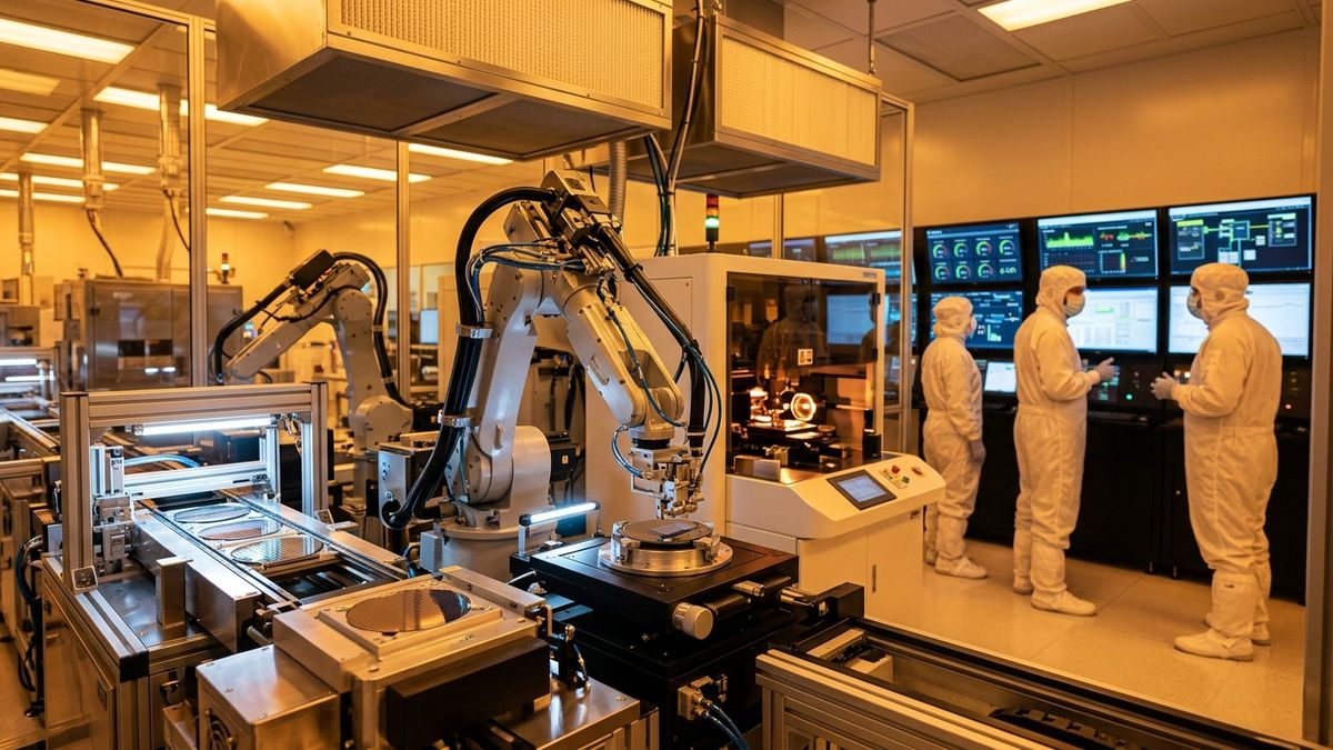
Aheesa Digital's VIHAAN chip achieved first-pass silicon success—a rare and critical milestone validating India's capacity for indigenous, production-ready semiconductor design.
Aheesa Digital has achieved first-pass silicon success for its VIHAAN chip—a landmark milestone in India's semiconductor journey that validates the country's growing capacity for indigenous, production-ready chip design. First-pass silicon success, where a chip functions correctly the very first time it is manufactured without requiring design revisions, is exceptionally rare and signals both engineering maturity and rigorous design verification methodology.
For context: industry estimates suggest that fewer than 30% of first-time silicon tape-outs achieve clean first-pass functionality. Aheesa Digital's success with VIHAAN places the startup in elite company—and sends a strong signal to global fabless semiconductor players considering India as a design hub.
What Is VIHAAN and Why Does It Matter?
VIHAAN is positioned as a purpose-built system-on-chip (SoC) targeting edge-compute and IoT connectivity use cases—markets experiencing explosive growth as AI workloads migrate from cloud to device. While detailed specifications remain under embargo pending commercialisation, the chip is understood to incorporate:
- Custom RISC-V based processing cores optimised for ultra-low-power inference
- Integrated wireless connectivity subsystem (supporting BLE 5.3 and Wi-Fi 6)
- On-chip security enclave with hardware root-of-trust
- Mixed-signal analog front-end for sensor interface applications
"First-pass success isn't just about this chip—it's proof that Indian engineers can execute the full-stack design, verification, and tape-out process to production standards,"said a semiconductor industry veteran familiar with the project. "VIHAAN is a flag in the ground for Indian fabless design."
The First-Pass Milestone: Why It's Technically Significant
Semiconductor design is an extraordinarily complex discipline where design errors can only be detected after manufacturing—a process that costs hundreds of thousands to millions of dollars per tape-out, depending on process node. The verification flow required to achieve first-pass success involves:
| Verification Stage | Description | Industry Pass Rate |
|---|---|---|
| Functional Simulation | RTL-level logic verification | ~95% achieve |
| Formal Verification | Mathematical proof of correctness | ~80% achieve |
| Physical Verification (DRC/LVS) | Layout rule & schematic matching | ~75% achieve |
| Timing Closure (STA) | Signal timing validation | ~60% achieve |
| First-Pass Silicon | Fully functional on first fabrication | ~25–30% achieve |
India's Semiconductor Design Ecosystem
Aheesa Digital's milestone arrives as India's semiconductor ecosystem undergoes its most significant transformation in decades. The India Semiconductor Mission (ISM), backed by a ₹76,000 crore incentive package, has catalysed both fab-side investments (Tata Electronics, CG Power-Renesas joint ventures) and fabless design activity.
Homegrown chip design startups including Mindgrove Technologies (Secure IoT chip), InCore Semiconductors (RISC-V), and now Aheesa Digital are building a credible Indian fabless IP portfolio—a prerequisite for India to graduate from being a chip consumer to a chip contributor.
Aheesa Digital's Roadmap
With first-pass silicon validated, Aheesa Digital is expected to accelerate commercialisation conversations with OEMs in the consumer electronics, industrial IoT, and smart infrastructure segments. The startup is also likely to use this milestone as a key fundraising catalyst, as verified silicon dramatically de-risks investor exposure compared to pre-tape-out ventures.
For deeper context on India's semiconductor ambitions, read our coverage on India's chip manufacturing milestones and RISC-V startups shaping Indian deep tech.