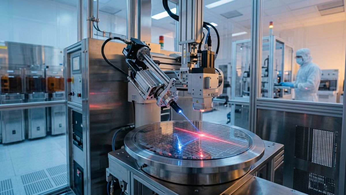
Indian deeptech startup Makr Microsystems raises ₹10.2 Crore in seed funding to advance semiconductor metrology, wafer defect detection, and domestic chip packaging equipment.
Executive Key Takeaways
- Indian deeptech startup Makr Microsystems raises ₹10.2 Crore in seed funding to advance semiconductor metrology, wafer defect detection, and domestic chip packaging equipment.
- A domestic semiconductor ecosystem cannot survive solely on imported cleanroom machinery, said senior semiconductor fabrication researchers tracking the venture. Without domestic intellectual property in metrology, defect classification, and precision stage actuation, fabs remain vulnerable to foreign supply disruptions and unsustainable capital expenditure overheads.
- Key Benchmark: **Defect Detection Sensitivity** — Sub-15nm Optical / E-Beam
CHENNAI — In a critical development for India's ambitions to build an indigenous semiconductor supply chain, deeptech hardware venture Makr Microsystems has secured ₹10.2 Crore ($1.22 million) in a seed funding round led by specialized deeptech venture funds, hardware angel syndicates, and prominent semiconductor industry veterans. The seed capital will be deployed to accelerate development of its proprietary precision optical metrology systems, automated wafer defect inspection tools, and advanced packaging verification hardware.
The fundraise comes at a pivotal juncture as the India Semiconductor Mission (ISM) gains operational momentum, with landmark commercial fabrication facilities and Outsourced Semiconductor Assembly and Test (OSAT) units breaking ground across Gujarat, Assam, and Tamil Nadu. Makr Microsystems addresses one of the most technologically demanding and capital-intensive segments of the semiconductor value chain: non-destructive yield metrology and sub-micron wafer defect inspection.
This technical breakthrough connects to the broader engineering modernization analyzed in The Agentic Shift in Indian IT and aligns with capital inflows tracked in RBI Operationalises Pre-Sanctioned Credit on UPI.
The Metrology Bottleneck: Why Precision Inspection Dictates Fab Economics
In modern semiconductor fabrication, a single 300mm silicon wafer undergoes hundreds of sequential chemical, photolithographic, etching, and deposition steps over a 60-to-90-day manufacturing cycle. A nanometer-scale particulate defect, layer overlay misalignment, or film thickness irregularity early in the fabrication sequence can ruin thousands of individual integrated circuit dies, destroying hundreds of thousands of dollars in commercial value.
Global metrology equipment is currently dominated by an oligopoly of multinational corporations such as KLA Corporation, Applied Materials, and ASML. For emerging semiconductor nations like India, relying entirely on foreign equipment vendors introduces long procurement lead times exceeding 18 to 24 months, geopolitical licensing restrictions, and exorbitant maintenance contracts.
"A domestic semiconductor ecosystem cannot survive solely on imported cleanroom machinery,"said senior semiconductor fabrication researchers tracking the venture. "Without domestic intellectual property in metrology, defect classification, and precision stage actuation, fabs remain vulnerable to foreign supply disruptions and unsustainable capital expenditure overheads."
Technical Specifications: Makr Microsystems Metrology Platform
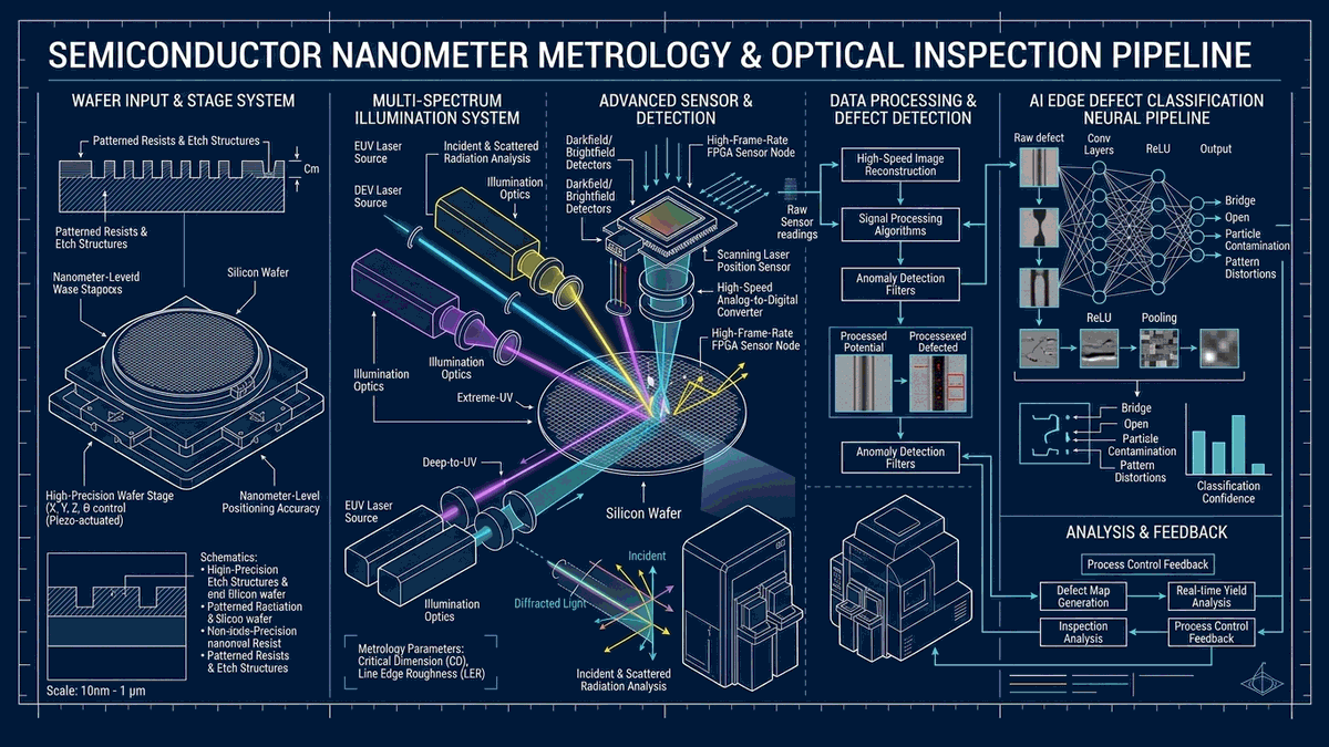
Makr Microsystems has engineered an advanced optoelectronic metrology platform tailored for compound semiconductors (Silicon Carbide and Gallium Nitride), advanced OSAT packaging inspection, and 200mm/300mm silicon wafer quality assurance. The platform combines deep-ultraviolet (DUV) laser scatterometry with high-speed interferometric sensors to achieve non-destructive surface topology mapping.
The table below outlines the core technical metrics of the Makr Microsystems platform compared to industry benchmarks:
| Metrology & Operational Parameter | Conventional Foreign Baseline (KLA / AMAT) | Makr Microsystems Platform | Strategic Fab Advantage |
|---|---|---|---|
| Defect Detection Sensitivity | Sub-15nm Optical / E-Beam | Sub-40nm Optical Brightfield & Darkfield | Optimized for Power Discretes & OSAT |
| Wafer Throughput Speed | 30 – 50 Wafers Per Hour (WPH) | 45 – 60 Wafers Per Hour (WPH) | High-Volume Packaging Line Integration |
| Substrate Compatibility | Standard Silicon (Si) Only | Silicon (Si), Silicon Carbide (SiC), GaN | Native Support for EV & Power Electronics |
| Stage Actuation Precision | 5nm Closed-Loop Piezo Stage | 10nm Multi-Axis Interferometric Stage | Proprietary Sub-Micron Motion Mechanics |
| Software Defect Classification | Proprietary Vendor Rule Engine | Deep Learning Multi-Class Defect Classifier | Instant Pattern Recognition & Yield Scoring |
| Equipment Capital Cost (CapEx) | $3.5M – $8.0M Per Tool | Estimated 60% CapEx Reduction | Democratizes Equipment for Indian OSATs |
| Procurement Lead Time | 14 – 22 Months Global Backlog | 4 – 6 Months Domestic Build Pipeline | Rapid Deployment for Indian Fabs |
Aligning With India's OSAT and ATMP Expansion
While cutting-edge sub-3nm logic fabs command headlines, the most immediate commercial demand in India's semiconductor landscape lies in Advanced Packaging, Testing, and Assembly (ATMP/OSAT), as well as wide-bandgap compound semiconductors powering electric vehicles and 5G telecommunications infrastructure. Facilities being established by the Tata Group, Micron Technology, and CG Power require thousands of quality verification steps per day.
Makr Microsystems has deliberately optimized its initial commercial toolset for:
- Through-Silicon Via (TSV) Depth Verification: Ensuring electrical interconnects in 2.5D and 3D chiplet packages meet precise micrometric depth tolerances.
- Solder Bump & Die-Attach Coplanarity: Detecting sub-micron tilt and void defects in flip-chip packaging before final resin encapsulation.
- SiC Wafer Epitaxial Defect Mapping: Identifying micro-pipe dislocations and basal plane defects in Silicon Carbide wafers used for high-voltage EV inverters.
R&D Roadmap and Pilot Line Commercialization
With the ₹10.2 Crore seed capital secured, Makr Microsystems will focus on finalizing field-testing units for cleanroom qualification across tier-one academic research fab lines and private packaging test facilities. The funding will also support expanding its multidisciplinary engineering team across optical physics, precision mechanical tooling, embedded FPGA programming, and computer vision.
As India's semiconductor ambitions transition from policy announcements to active silicon fabrication, ventures like Makr Microsystems prove that domestic entrepreneurs are willing to tackle the deepest, most complex hardware layers underpinning modern digital civilization.