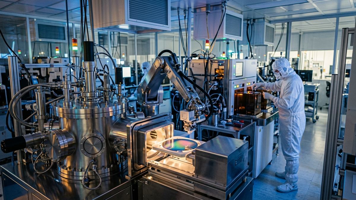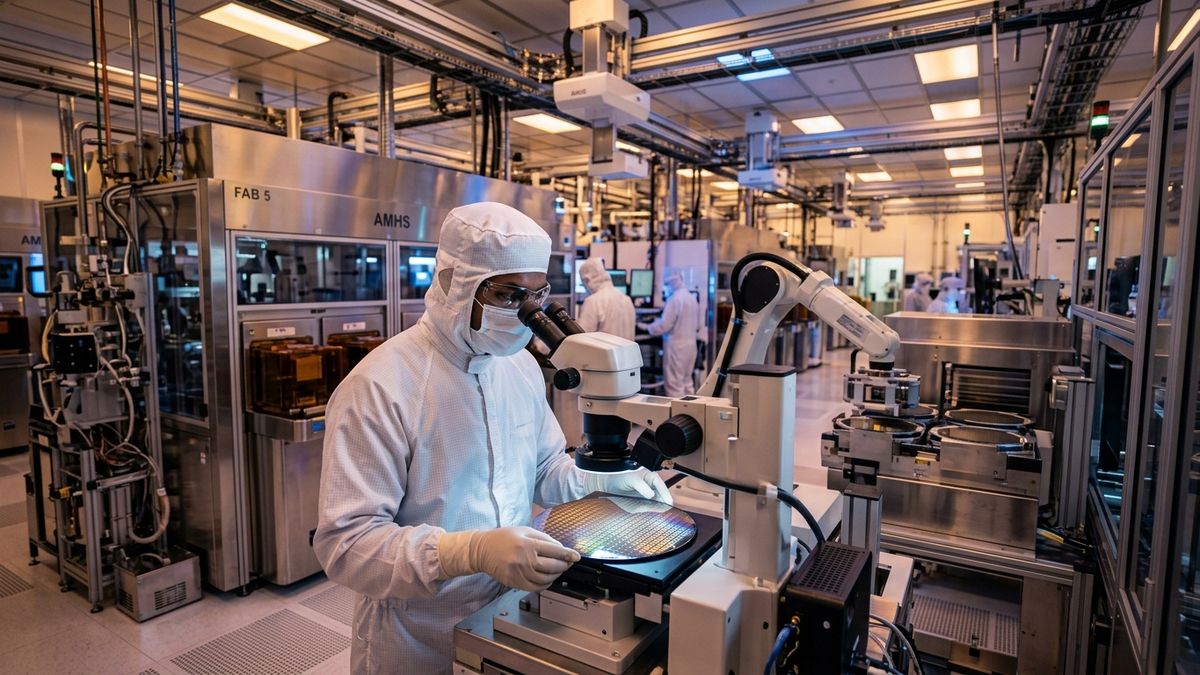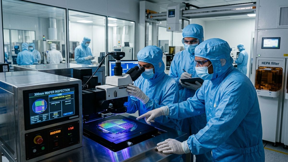
Under the expanded Semicon 2.0 blueprint, India is building a massive specialized talent pipeline of 100,000 VLSI chip designers, cleanroom operators, and ATMP packaging engineers across top universities and global fab partnerships.
Executive Key Takeaways
- Under the expanded Semicon 2.0 blueprint, India is building a massive specialized talent pipeline of 100,000 VLSI chip designers, cleanroom operators, and ATMP packaging engineers across top universities and global fab partnerships.
- Hardware manufacturing is unforgiving; a single particulate contamination or sub-nanometer alignment error can destroy entire wafer lots, said senior advisors to the India Semiconductor Mission. Semicon 2.0 is not merely about subsidized industrial infrastructure—it is about establishing a self-sustaining intellectual ecosystem that transforms India from a chip consumer into a premier silicon design and manufacturing hub.
- Key Benchmark: **Front-End Fab Engineering** — 25,000
NEW DELHI — In an aggressive expansion of the national deeptech roadmap, the Government of India has unveiled the talent mandate under Semicon 2.0, aiming to train and certify over 100,000 specialized semiconductor engineers, VLSI designers, and cleanroom fabrication technicians by 2030.
The initiative represents the human capital backbone of the $15+ billion India Semiconductor Mission (ISM). With commercial fabrication facilities, outsourced assembly and testing (OSAT) units, and compound semiconductor plants breaking ground across Gujarat, Assam, Karnataka, and Tamil Nadu, the demand for certified chip architects, process engineers, and lithography specialists is reaching unprecedented levels.
This sweeping human capital rollout complements strategic hardware milestones highlighted in Infineon Acquires Bengaluru Chip Startup C2i Semiconductors to Supercharge AI Data Centre Power Management and the advanced optoelectronics push covered in ₹70 Crore National Programme Accelerates India’s Strategic Photonics Tech with Olee.space as Fabrication Partner.
Bridging the Cleanroom Skill Gap: Inside the Multi-Tier Training Pipeline
While India has historically accounted for nearly 20% of the world's fabless chip design workforce—housing major R&D centers for Nvidia, Qualcomm, Intel, and Texas Instruments—domestic expertise in physical wafer fabrication, chemical deposition, plasma etching, and high-density advanced packaging has remained limited.
The Semicon 2.0 human capital framework addresses this asymmetry through a structured multi-tiered training architecture:
1. Category A: Advanced VLSI & EDA Architecture: 30,000 postgraduate and undergraduate engineers trained in custom ASIC design, RISC-V sovereign cores, hardware security, and EDA software pipelines from Synopsys, Cadence, and Siemens EDA.
2. Category B: Cleanroom & Lithography Process Engineering: 40,000 certified technicians and diploma engineers specializing in sub-28nm process flows, chemical mechanical planarization (CMP), extreme ultraviolet (EUV) calibration, and high-purity gas handling.
3. Category C: Advanced Packaging (ATMP & OSAT): 30,000 engineers dedicated to 2.5D/3D chiplet integration, high-density substrate manufacturing, thermal dissipation, and automated optical inspection (AOI).
"Hardware manufacturing is unforgiving; a single particulate contamination or sub-nanometer alignment error can destroy entire wafer lots,"said senior advisors to the India Semiconductor Mission. "Semicon 2.0 is not merely about subsidized industrial infrastructure—it is about establishing a self-sustaining intellectual ecosystem that transforms India from a chip consumer into a premier silicon design and manufacturing hub."
Semicon 2.0 Human Capital Allocation & Skill Development Matrix
The structured table below details the educational allocation, institutional partners, and technical competencies targeted under the program:
| Semiconductor Domain | Target Workforce | Primary Academic Hubs | Core Technical Curriculum |
|---|---|---|---|
| Front-End Fab Engineering | 25,000 | IIT Bombay, IIT Madras, SCL Mohali | Wafer lithography, thin-film deposition, wet chemistry, vacuum physics |
| VLSI & System-on-Chip Design | 35,000 | IIT Hyderabad, BITS Pilani, NIT Trichy | Verilog/VHDL, RISC-V synthesis, place-and-route, physical verification |
| ATMP & Advanced Packaging | 25,000 | IIT Roorkee, Anna University, MSMEs | Ball grid array (BGA), wire bonding, epoxy mold underfill, thermal testing |
| Compound Semiconductors & GaN | 15,000 | IISc Bengaluru, IIT Delhi, CeNSE | Gallium Nitride (GaN), Silicon Carbide (SiC) power switching, RF modules |
Academic-Industry Integration: EDA Tool Access and Living Fab Labs
A cornerstone of Semicon 2.0 is the complete elimination of licensing cost barriers for Indian universities. Over 120 engineering institutions have been granted direct, subsidized access to commercial-grade electronic design automation (EDA) software suites.
Furthermore, students are provided tape-out subsidies, allowing top engineering teams to manufacture their custom silicon designs at the Semi-Conductor Laboratory (SCL) in Mohali and partner international commercial foundries. By bridging theoretical circuit design with hands-on silicon prototyping, India is creating a resilient engineering workforce capable of sustaining national high-tech independence for decades to come.