Under a ₹70 Crore national strategic deeptech initiative, Olee.space is selected as Development-cum-Production Partner to advance integrated silicon photonics, optical interconnects, and space communications.
Executive Key Takeaways
- Under a ₹70 Crore national strategic deeptech initiative, Olee.space is selected as Development-cum-Production Partner to advance integrated silicon photonics, optical interconnects, and space communications.
- Integrated photonics is the defining semiconductor frontier of the 21st century, serving as the foundational bedrock for next-generation AI hyperscale data centres, quantum encryption, and space-to-ground laser communications, stated senior scientific leadership overseeing the strategic mission. Designating Olee.space as our Development-cum-Production Partner establishes a robust sovereign fabrication pipeline, ensuring India develops domestic intellectual property across every phase of optical wafer packaging and testing.
- Key Benchmark: **Data Throughput** — 10 – 40 Gbps per channel
BENGALURU & NEW DELHI — In a major breakthrough for India's sovereign semiconductor and quantum technologies roadmap, the Government of India has sanctioned a ₹70 Crore ($8.4 million) Advanced Photonics Technology Programme, officially selecting deeptech venture Olee.space as its primary Development-cum-Production Partner (DcPP).
The strategic programme is mandated to transition domestic Photonic Integrated Circuit (PIC) designs, optical interconnects, and satellite optical communications payloads from laboratory-scale prototypes into qualified, fabrication-ready commercial production. By utilizing light (photons) instead of electrical current (electrons) to process and transmit data across silicon micro-chips, photonics technology provides orders-of-magnitude improvements in data throughput, thermal dissipation, and electromagnetic immunity.
The development reinforces India’s sovereign hardware and deeptech design push documented in Infineon Acquires Bengaluru Chip Startup C2i Semiconductors to Supercharge AI Data Centre Power Management and strengthens the aerospace testing infrastructure analyzed in India’s Space-Tech Startups Push for Dedicated ‘Space City’ Hub in Telangana to Accelerate Testing and Manufacturing.
The Optical Computing Revolution: Why Silicon Photonics Is Indispensable
As artificial intelligence computing clusters and high-bandwidth satellite constellations expand exponentially, traditional copper-based electrical interconnects have encountered insurmountable physical limitations. In advanced AI server racks and inter-satellite links, copper traces suffer from severe high-frequency attenuation, capacitive signal degradation, and massive thermal power dissipation.
Silicon photonics integrates optical laser sources, modulators, optical waveguides, and photodetectors directly onto microchips fabricated with standard CMOS semiconductor processes.
Key technical advantages unlocked by integrated photonics include:
1. Light-Speed Bandwidth Density: Optical waveguides transmit multiple wavelengths of light simultaneously (dense wavelength division multiplexing or DWDM) over a single microscopic fiber or silicon channel, scaling data throughput to terabits per second.
2. Sub-Picojoule Power Consumption: Slashing power consumption per transmitted bit from ~15 pJ/bit in copper interconnects to under 1.5 pJ/bit in co-packaged optics (CPO).
3. Space-Hardened Immunity: In space and aerospace environments, optical communications are completely impervious to electromagnetic interference (EMI), solar radiation bursts, and radio-frequency spoofing.
"Integrated photonics is the defining semiconductor frontier of the 21st century, serving as the foundational bedrock for next-generation AI hyperscale data centres, quantum encryption, and space-to-ground laser communications,"stated senior scientific leadership overseeing the strategic mission. "Designating Olee.space as our Development-cum-Production Partner establishes a robust sovereign fabrication pipeline, ensuring India develops domestic intellectual property across every phase of optical wafer packaging and testing."
Comparative Architecture and Strategic Benchmark Matrix
Under the ₹70 Crore initiative, Olee.space will lead the commercialization of specialized Photonic Integrated Circuits across defense, aerospace, and high-performance computing (HPC) domains. The table below delineates the structural performance advantages of integrated silicon photonics compared to conventional copper and radio-frequency (RF) systems:
| Architectural Metric | Conventional Copper / RF Interconnects | Integrated Silicon Photonics (Olee.space) | Strategic Advantage for India |
|---|---|---|---|
| Data Throughput | 10 – 40 Gbps per channel | 400 – 1,600+ Gbps (1.6 Tbps) | 40x throughput increase for AI training clusters |
| Energy Efficiency | 12 to 20 pJ / bit | < 1.8 pJ / bit | 85% reduction in data centre optical transceiver heat |
| Interconnect Reach | < 3 meters without signal repeaters | > 2,000 meters without degradation | Seamless optical disaggregation across entire server halls |
| Space Communications | Heavy RF antennas (50–120 kg) | Micro-Optic Laser Terminals (< 8 kg) | 70% payload weight reduction for LEO satellites |
| Electromagnetic Immunity | Highly vulnerable to EMI & jamming | 100% Dielectric Immune to EMI | Mission-critical secure quantum key distribution (QKD) |
Fabrication Pipeline, Packaging Cleanrooms, and Future Commercialization
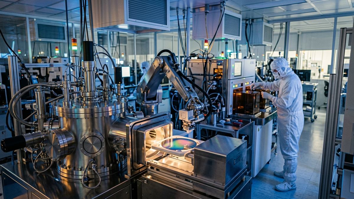
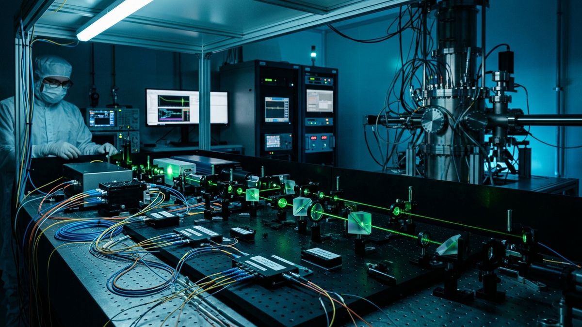
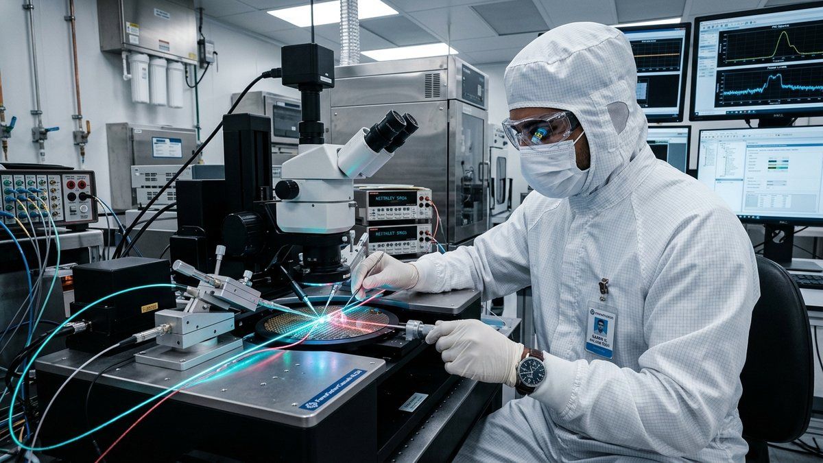
The ₹70 Crore capital deployment will establish dedicated automated optical probe stations, sub-micron die-attach packaging cleanrooms, and high-frequency electro-optic test benches in Bengaluru.
Olee.space will collaborate with Indian academic cleanroom facilities and commercial packaging foundries to deliver qualified optical transceiver modules and free-space optical (FSO) satellite communication terminals. By successfully moving integrated photonics from laboratory proof-of-concept to volume manufacturing, India is establishing sovereign technological supremacy in one of the most critical high-tech hardware domains of the decade.