AI Could Supercharge India's Chip Ambitions: Cadence Highlights Automated Verification Edge
By Karthik Ramaswamy | Published August 18, 2026 | 7 min read

Cadence Design Systems reveals how AI-driven chip design and automated verification can slash semiconductor development cycles, unlocking a massive strategic edge for India.
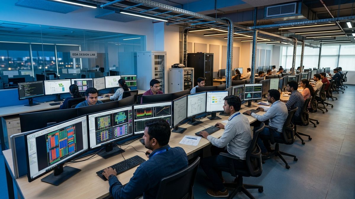
The convergence of generative artificial intelligence and electronic design automation (EDA) is poised to fundamentally accelerate India's semiconductor journey, according to senior technologists at EDA industry giant Cadence Design Systems. By automating complex VLSI layout routing, timing closure, and functional bug detection, AI-augmented design workflows are slashing chip development cycles from 24 months down to under 9 months.
This technological breakthrough creates an unprecedented window of opportunity for India, which already houses over 125,000 semiconductor design engineers—representing nearly 20% of the world's fabless chip design workforce across Bengaluru, Hyderabad, Noida, and Pune.
Overcoming the Silicon Verification Bottleneck
In modern semiconductor design at advanced sub-7nm process nodes, functional verification consumes upwards of 60% to 70% of total engineering hours and over 50% of the total design budget. A single uncaught hardware bug discovered after silicon fabrication can cost over $50 million in mask re-spins and delay market entry by a year.
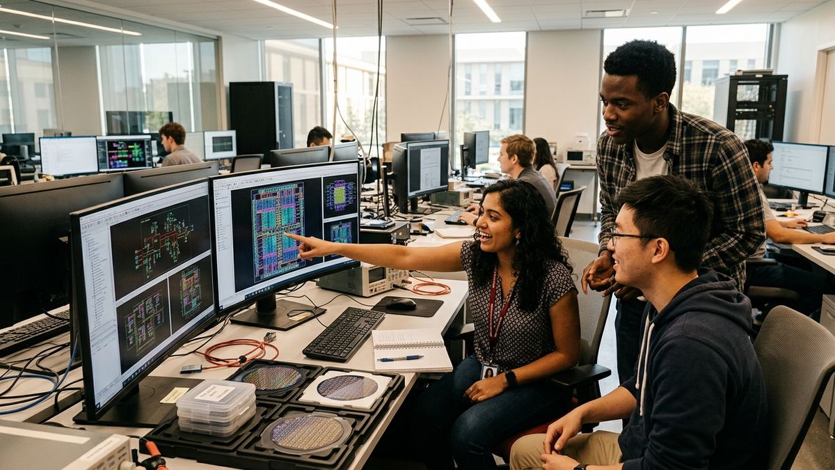
By integrating reinforcement learning, graph neural networks (GNNs), and LLM-driven testbench generators, AI EDA tools allow design teams to uncover edge-case regressions orders of magnitude faster than human verification teams.
| Semiconductor Design Phase | Traditional EDA Workflow | AI-Augmented EDA Flow (Cadence Cerebrus & JedAI) | Impact on Indian Design Teams |
|---|---|---|---|
| RTL Architecture & Coding | Manual Verilog/VHDL writing | LLM-assisted RTL generation & linting | 3x Faster initial drafting |
| Functional Verification | Manual testbench writing & random testing | Autonomous agentic test coverage synthesis | 5x Faster coverage closure |
| Place and Route (P&R) | Iterative manual floorplanning | Reinforcement learning optimization | 15%–20% PPA (Power/Performance/Area) gain |
| Timing Closure & Signoff | Multi-week manual static timing analysis | Neural-network-accelerated timing prediction | 70% reduction in signoff turnaround |
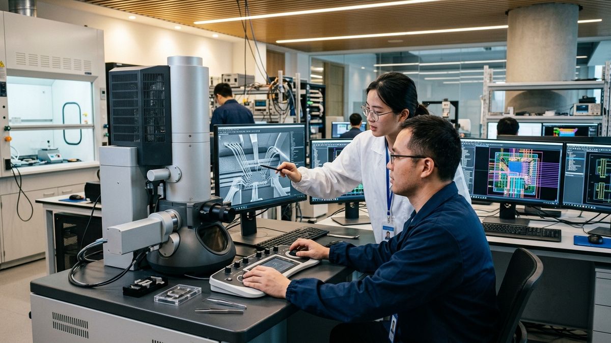
| Silicon Bring-Up | Lab bench manual debugging | Automated telemetry diagnosis | Weeks instead of months |
Why India Holds a Natural Competitive Advantage
India's semiconductor ecosystem stands to benefit disproportionately from AI-driven EDA transformation for several key reasons:
"India is not starting from zero in semiconductors—it has been the design engine of the world for thirty years,"explained a Cadence senior technical director. "With AI automating routine floorplanning and verification tasks, Indian engineers can elevate from execution partners to architects of proprietary, high-value domain-specific silicon."
1. Massive Pre-Existing VLSI Talent Pool
Global semiconductor giants—including Intel, AMD, Qualcomm, NVIDIA, Texas Instruments, and MediaTek—conduct major portions of their core tape-outs in Indian R&D centers. Indian engineers are already the primary users of next-generation EDA software suites.
2. Rise of Indigenous Fabless Startups
Startups such as Mindgrove Technologies, InCore Semiconductors, and Aheesa Digital with its VIHAAN chip are leveraging AI EDA tools to execute tape-outs with lean engineering teams of 15–30 engineers, rivaling legacy corporate teams of hundreds.
3. Synergies with Domestic Manufacturing
As India operationalizes 12 major semiconductor fab and OSAT facilities worth ₹1.64 lakh crore, local fabless designs can be seamlessly handed off to domestic packaging plants.
Strategic Implications for India's Tech Sovereignty
Integrating AI into semiconductor design ensures that India can develop sovereign chips for critical applications—ranging from defense and telecommunications to electric vehicle mobility platforms.
Combined with surging capital inflows into deep-tech AI startups, the marriage of artificial intelligence and chip architecture will serve as the bedrock of India's trillion-dollar digital economy.