India's Semiconductor Push Accelerates: 12 Projects Worth ₹1.64 Lakh Crore Approved as Production Begins
By Sanjay Patel | Published August 18, 2026 | 7 min read

India has approved 12 semiconductor projects totaling ₹1.64 lakh crore with three units now operational, shifting the nation from strategic blueprints to commercial chip fabrication.
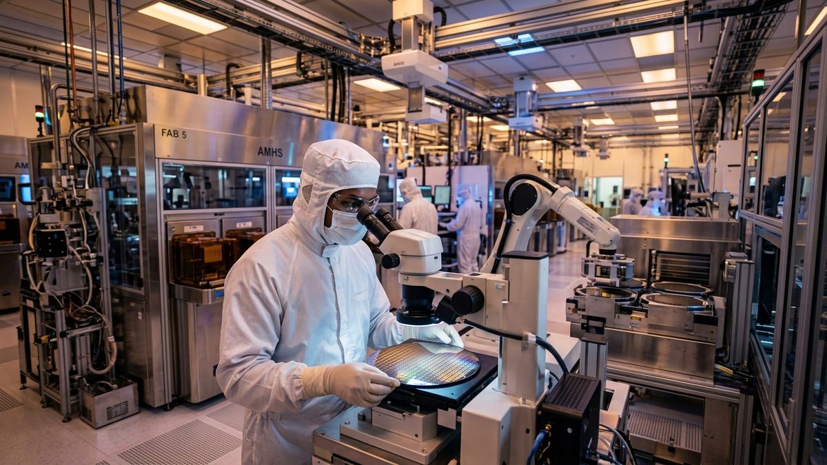
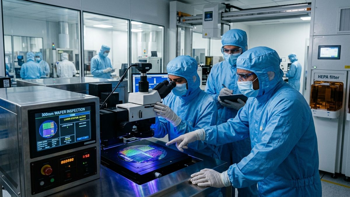
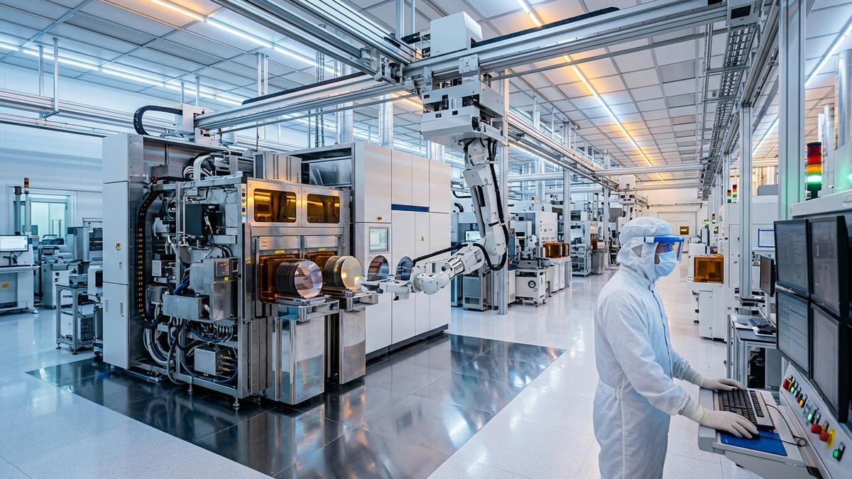
India has crossed a definitive threshold in its technological industrialization journey, with the Union Government approving 12 semiconductor projects representing an aggregate capital commitment of ₹1.64 lakh crore (approximately $19.7 billion). Crucially, three assembly, testing, marking, and packaging (ATMP) and pilot fabrication facilities have now transitioned from construction to live operational status, marking the start of commercial silicon processing on Indian soil.
The acceleration reflects the compounding momentum of the India Semiconductor Mission (ISM), launched with an initial ₹76,000 crore fiscal incentive outlay. By establishing domestic packaging and fabrication capabilities, India is seeking to insulate its high-growth electronics manufacturing sector from geopolitical supply chain bottlenecks while positioning the domestic ecosystem as a trusted node in the global silicon supply chain.
The Transition: From Capital Subsidies to Operational Wafers
For decades, India excelled in fabless semiconductor design—housing over 20% of the world's VLSI design engineers—while remaining entirely dependent on East Asia for physical chip fabrication and packaging. The operationalization of the first three semiconductor facilities under the ISM umbrella fundamentally alters this dynamic.
The approved projects span full-scale commercial wafer fabs, advanced OSAT (Outsourced Semiconductor Assembly and Test) units, and compound semiconductor facilities targeting electric vehicles, telecommunications, and defense electronics.
| Project Venture | Partner Entities | Location | Committed Investment | Focus & Node Capability | Status |
|---|---|---|---|---|---|
| Tata Electronics Fab | Powerchip (PSMC, Taiwan) | Dholera, Gujarat | ₹91,000 Cr ($11B) | 28nm, 40nm, 90nm Logic Chips | Under Rapid Construction |
| Tata OSAT Facility | Tata Semiconductor Assembly | Jagiroad, Assam | ₹27,000 Cr ($3.2B) | Advanced Flip-Chip & 2.5D Packaging | Operational / Scaling |
| CG Power-Renesas OSAT | Renesas (Japan) & Stars Micro (Thailand) | Sanand, Gujarat | ₹7,600 Cr ($910M) | Legacy & Automotive Power ICs | Operational / Phase-1 Live |
| Micron Technology ATMP | Micron Technology (USA) | Sanand, Gujarat | ₹22,500 Cr ($2.7B) | DRAM & NAND Flash Memory Modules | Operational / Phase-1 Cleanroom |
| Kaynes Semicon OSAT | Kaynes Technology | Sanand, Gujarat | ₹3,300 Cr ($400M) | Power Modules & Smart Meter ICs | Commissioning |
| Suchi Semicon | Domestic Consortium | Surat, Gujarat | ₹840 Cr ($100M) | Discrete Semiconductors & Sensors | Commissioning |
Strategic Significance: De-Risking the Electronics Supply Chain
India's domestic electronics production expanded past $115 billion in FY2025, driven by smartphone assembly, automotive electronics, and industrial automation. However, semiconductor components accounted for nearly $35 billion in import bills.
"Transitioning from paper MoUs to cleanroom operations in under 24 months is a testament to extraordinary coordination between central agencies and state infrastructure teams,"stated an ISM senior advisory board member. "Having three operational facilities producing packaged silicon proves that India can execute world-class semiconductor infrastructure at scale."
The Multiplier Effect on Ancillary Industries
The operationalization of semiconductor units is triggering immediate spillover investments across specialized supply chain tiers:
1. Ultra-Pure Gases and Specialty Chemicals: Leading industrial gas suppliers like Linde, Air Liquide, and Inox Air Products are co-locating high-purity nitrogen, argon, and silane production units adjacent to semiconductor clusters.
2. Cleanroom Engineering and Substrates: Domestic engineering conglomerates are mastering cleanroom HVAC standards of ISO Class 1 to Class 1000, establishing local engineering mastery.
3. Talent Incubation Pipeline: Over 100 Indian universities have integrated cadence and synopsys EDA toolsuites into their undergraduate curriculum to graduate 85,000 industry-ready VLSI and packaging engineers by 2028.
Addressing the Fabless-to-Fab Integration
While manufacturing infrastructure expands, Indian fabless startups are capturing unprecedented value by designing custom chips destined for domestic packaging lines.
As demonstrated by recent breakthroughs such as Aheesa Digital's VIHAAN chip milestone, domestic design teams now have direct pathways to validate and package silicon without long cross-border logistics delays. Furthermore, the integration of AI-powered automated verification tools is shrinking development cycles from quarters to weeks.
Supported by targeted state incentives like the Haryana startup incentives package and Gujarat's dedicated semiconductor industrial corridors, India's chip ecosystem is establishing the resilient infrastructure needed for global competitiveness.