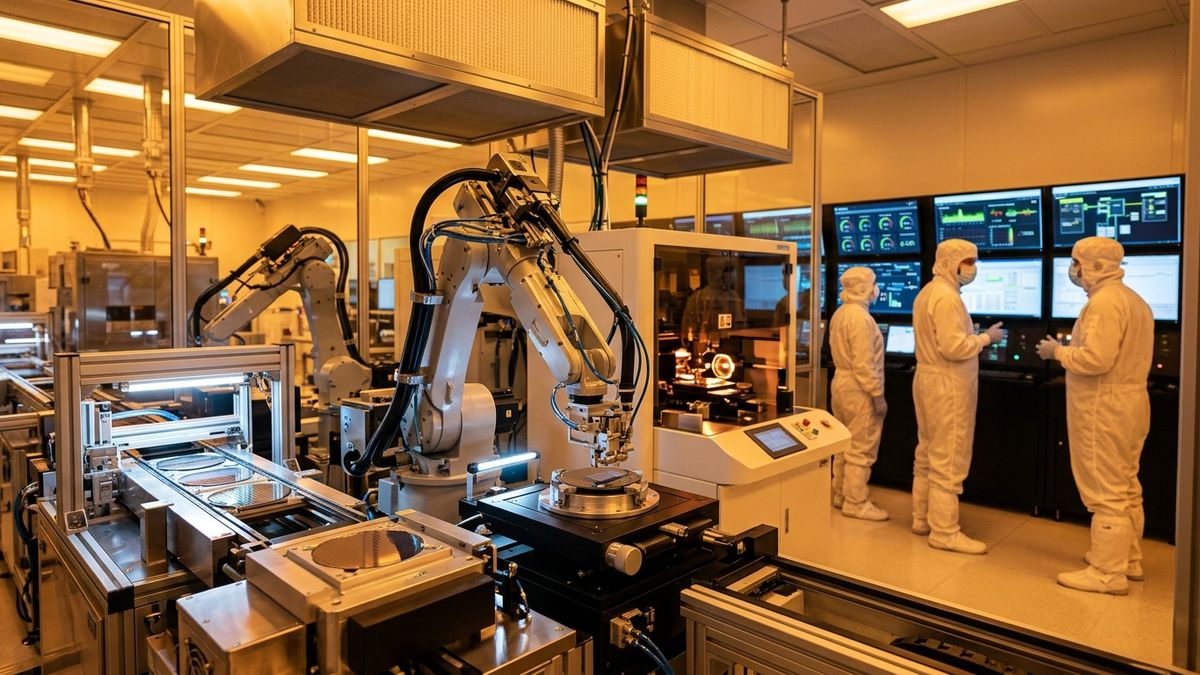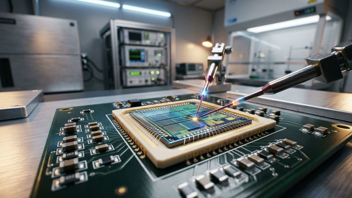
ASIP Technologies is building a state-of-the-art ₹2,500 Crore semiconductor assembly, testing, and packaging (OSAT) facility in Visakhapatnam, boosting India's chip manufacturing self-reliance.
Executive Key Takeaways
- ASIP Technologies is building a state-of-the-art ₹2,500 Crore semiconductor assembly, testing, and packaging (OSAT) facility in Visakhapatnam, boosting India's chip manufacturing self-reliance.
- The battle for global semiconductor supremacy is no longer fought solely in multi-billion dollar cleanroom foundries; it is increasingly won or lost on the advanced packaging floor, declared a senior director at ASIP Technologies during the Visakhapatnam ground-breaking ceremony. Our ₹2,500 Crore OSAT facility bridges the vital link between fabless chip designers and finished electronic devices, ensuring that India captures the high-margin, high-complexity assembly value chain locally.
- Key Benchmark: **Capital Expenditure Intensity** — Extreme ($8B – $15B per cleanroom fab)
VISAKHAPATNAM — In a milestone investment that solidifies India’s ascent as a premier global microelectronics hub, ASIP Technologies has officially broken ground on its state-of-the-art ₹2,500 Crore ($300 Million) semiconductor packaging, assembly, and testing (OSAT) facility in Visakhapatnam, Andhra Pradesh.
Backed by central incentives under the India Semiconductor Mission (ISM) and state industrial subsidies, the mega-facility is designed to provide advanced Outsourced Semiconductor Assembly and Test (OSAT) services, including high-density flip-chip ball grid arrays (FCBGA), 2.5D/3D heterogeneous chiplet integration, and system-in-package (SiP) modules. The Visakhapatnam plant will cater to soaring domestic and international demand across automotive electronics, 5G/6G telecom baseband processors, industrial automation, and consumer electronics.
This groundbreaking follows massive recent domestic semiconductor milestones, including global buyouts detailed in Infineon Acquires Bengaluru-Based C2i Semiconductors and extraterrestrial silicon deployment examined in Made-in-India Chips Power Major Space Missions.
Why Advanced Packaging Is the True Frontier of Moore’s Law
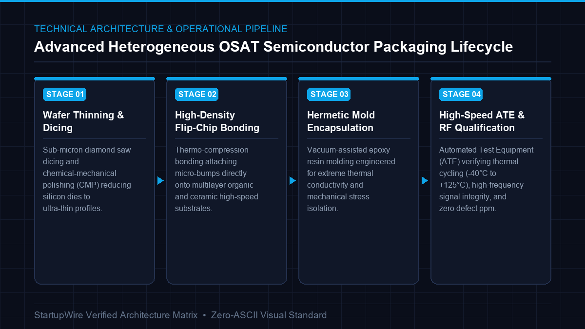
As traditional front-end semiconductor fabrication approaches atomic physical limits—making sub-2nm silicon wafer manufacturing exponentially expensive—the global semiconductor industry has pivoted toward Advanced Packaging and Heterogeneous Integration.
Rather than attempting to fabricate an entire monolithic microprocessor onto a single fragile die, advanced OSAT facilities take multiple specialized modular "chiplets" (e.g., an optical memory chip from one fab, a 5nm logic core from another, and an analog power regulator from a third) and interconnect them with sub-micron pitch copper pillars on a single high-performance substrate.
"The battle for global semiconductor supremacy is no longer fought solely in multi-billion dollar cleanroom foundries; it is increasingly won or lost on the advanced packaging floor,"declared a senior director at ASIP Technologies during the Visakhapatnam ground-breaking ceremony. "Our ₹2,500 Crore OSAT facility bridges the vital link between fabless chip designers and finished electronic devices, ensuring that India captures the high-margin, high-complexity assembly value chain locally."
Semiconductor Value Chain Economics: Wafer Fab vs. Advanced OSAT vs. Pure Assembly
The financial and operational distinction between microelectronics manufacturing layers is detailed in the comparative matrix below:
| Manufacturing Vertical | Front-End Silicon Wafer Fab (e.g. TSMC / Tata) | Advanced Heterogeneous OSAT (ASIP Technologies) | Legacy Low-End Assembly (PCB SMT) |
|---|---|---|---|
| Capital Expenditure Intensity | Extreme ($8B – $15B per cleanroom fab) | Moderate ($300M – $800M per facility) | Low ($10M – $30M per assembly line) |
| Cleanroom Classification | ISO Class 1 (Sub-atomic dust control) | ISO Class 100 to Class 1,000 (Ultra-Clean Precision) | ISO Class 10,000 to Class 100,000 |
| Time to First Commercial Revenue | 48 – 60 Months (Lengthy qualification) | 18 – 24 Months (Fast commercial ramp) | 6 – 12 Months |
| Core Intellectual Property | Extreme Ultraviolet (EUV) Lithography | Micro-Bump Bonding, 2.5D Interposers, SiP Architecture | Surface Mount Pick-and-Place Soldering |
| Gross Margin Profile | 45% – 55% | 28% – 38% (High-Margin Value Addition) | 8% – 14% (Commoditized contract margins) |
| Geopolitical Chokepoint Status | Extreme (Concentrated in Taiwan & Korea) | High (Historically dominated by Malaysia & Taiwan) | Low (Globally dispersed) |
Transforming Visakhapatnam into India’s Silicon Coast
The selection of Visakhapatnam as the hub for ASIP’s mega-facility offers strategic logistical advantages:
1. Direct Deep-Water Port Access: Immediate maritime shipping routes connecting East Asian silicon wafer foundries with Indian manufacturing corridors.
2. Reliable High-Voltage Power & Ultrapure Water: Continuous industrial utility infrastructure vital for sensitive chiplet packaging yields.
3. Deep Talent Pipeline: Premier engineering talent emerging from Andhra University, IIT Tirupati, and regional microelectronics vocational centers.
As analyzed in Semicon India Unites Global Chip Ecosystem, ASIP Technologies’ ₹2,500 Crore packaging plant establishes the indispensable hardware foundation that transforms India from a chip consumer into a sovereign semiconductor export superpower.