SEMICON India 2026 Gathers 500+ Exhibitors and Global Giants to Build End-to-End Sovereign Semiconductor Ecosystem
By Karthik Ramaswamy | Published August 20, 2026 | 8 min read
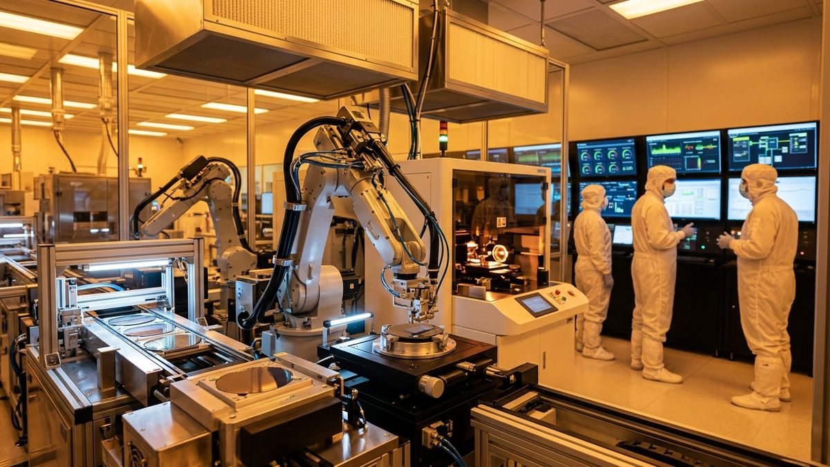
SEMICON India 2026 convenes 500+ exhibitors and 40+ national delegations at Yashobhoomi, accelerating Semicon 2.0 across fab construction, ATMP packaging, and specialized chemicals.
NEW DELHI — In a landmark milestone for India's high-technology manufacturing ambitions, SEMICON India 2026 is scheduled to convene from September 17 to 19, 2026, at the state-of-the-art Yashobhoomi (India International Convention & Expo Centre) in New Delhi. Co-organized by the India Semiconductor Mission (ISM) and global industry association SEMI, the flagship summit will bring together more than 500 exhibitors, 290 international corporations, and official delegations from over 40 countries, representing the complete global semiconductor value chain from silicon design and chemical synthesis to advanced front-end fabrication and OSAT/ATMP packaging.
To be inaugurated by Prime Minister Narendra Modi, the 2026 edition—themed "Silicon to Systems: Building the Ecosystem"—marks the formal operational acceleration of Semicon 2.0. Building upon the 12 commercial projects approved under the initial ₹76,000-crore incentive package (three of which have already commenced pilot and commercial production), the summit will focus on establishing domestic manufacturing for critical consumables, ultra-pure gases, photoresists, and compound semiconductors.
Global Participation and Country Pavilion Architecture
Spanning over 18,000 square meters of exhibition space, SEMICON India 2026 reflects unprecedented international commitment to diversifying the global semiconductor supply chain through Indian partnerships.
The exhibition floor will feature six dedicated international country pavilions, bringing together equipment manufacturers, materials suppliers, and research consortiums:
- Japan: Precision photolithography optics, wafer transport robotics, and specialized chemical purifiers.
- South Korea: Memory packaging architectures, high-purity silicon substrate manufacturing, and inspection gear.
- Singapore: Advanced testing, cleanroom engineering, and logistics supply chain hubs.
- Malaysia: World-class OSAT (Outsourced Semiconductor Assembly and Test) operational expertise.
- Germany: Precision laser tooling, industrial automation, and silicon carbide (SiC) power electronics.
- The Netherlands: Extreme Ultraviolet (EUV) and Deep Ultraviolet (DUV) lithography ecosystem suppliers and precision motion systems.
In addition, 10 Indian state government pavilions—including Gujarat, Karnataka, Tamil Nadu, Assam, Uttar Pradesh, Odisha, and Maharashtra—will compete to attract semiconductor fab investments, offering dedicated clean water pipelines, uninterrupted 220kV power substations, and tailored state capital subsidies.
From Semicon 1.0 to Semicon 2.0: The Ecosystem Maturation
While the initial phase of the India Semiconductor Mission succeeded in anchoring mega-fabs and multi-billion-dollar packaging plants—including Tata Electronics' 300mm wafer fab in Dholera and ATMP facility in Jagiroad, Assam, along with Micron's testing unit in Sanand—Semicon 2.0 addresses the critical supply chain dependencies required to sustain these mega-plants.
A semiconductor fab cannot operate in isolation. It requires an unbroken, secure supply of ultra-pure water (18.2 MΩ·cm resistivity), bulk industrial gases (ultra-high purity Nitrogen, Argon, Helium), electronic-grade acids, quartzware, silicon wafers, and precision calibration tooling.
"A semiconductor plant is not just a building with machines; it is a complex living ecosystem that requires thousands of specialized suppliers working with zero-defect tolerances,"emphasized ISM leadership. "SEMICON India 2026 is specifically structured to anchor the Tier-2 and Tier-3 chemical, gas, and tooling manufacturers in India so our foundries have sovereign supply-chain security."
Value Chain Breakdown: India Semiconductor Ecosystem Architecture
The table below outlines the multi-tiered architecture of the Indian semiconductor roadmap being showcased at SEMICON India 2026:
| Value Chain Segment | Primary Ecosystem Focus | Strategic Key Players & Partners | Domestic Infrastructure Status |
|---|---|---|---|
| 1. Front-End Fabrication | 28nm/40nm/65nm Logic, Compound GaN/SiC Fabs | Tata Electronics, PSMC, CG Power, Renesas | Dholera & Sanand mega-fabs under active construction |
| 2. Advanced ATMP / OSAT | 2.5D/3D Packaging, Fan-out wafer-level packaging, Flip-chip | Micron, Tata Jagiroad, Kaynes Semicon, Murata | First commercial packaging lines operational in 2026 |
| 3. IC Design & Verification | RISC-V architectures, AI ASIC accelerators, Automotive SoCs | 20% Global Design Workforce, C-DAC (VEGA/DIR-V) | Over 150,000 active semiconductor design engineers |
| 4. Specialty Materials & Gases | Ultra-pure chemicals, Electronic-grade gases, Quartz | Air Liquide, Linde, Domestic Chemical Consortia | Dedicated gas corridors in Dholera & Sanand clusters |
| 5. Equipment & Cleanrooms | ISO Class 1 cleanrooms, Automated Material Handling (AMHS) | SEMI Consortium, Global Tooling Vendors | Cleanroom engineering localized across 5 states |
Synergies with Sovereign Defense, Aerospace, and Quantum Tech
The rapid maturation of India's semiconductor manufacturing ecosystem has direct positive spillover effects into strategic sovereign industries, including aerospace, defense electronics, and quantum computing.
For instance, strategic partnerships like the Bharat Electronics (BEL) and Ananth Technologies defense aerospace MoU rely heavily on domestically packaged radiation-hardened integrated circuits and radar transceiver modules. Similarly, breakthrough deeptech ventures such as the QpiAI Quantum Foundry in Karnataka and defense sensor developments by Techno Defence's miniature cryocooler systems demonstrate how domestic fabrication and packaging capabilities empower high-spec engineering sectors.
Furthermore, GCC technology hubs like Charles Schwab's 2,000-engineer Hyderabad Center are increasingly building localized hardware-software verification teams to support mission-critical enterprise systems.
Conference Tracks, Talent Pipeline, and Startup Pitch Hackathons
Beyond the commercial expo, SEMICON India 2026 will feature over 150 globally renowned speakers across six specialized conference tracks:
1. Advanced Manufacturing & Node Scaling: Exploring 28nm mature nodes, Silicon Photonics, and Gallium Nitride (GaN) power devices for electric vehicles and data center power supplies.
2. AI & Digital Fab Automation: Implementing AI-driven predictive maintenance, defect detection, and automated wafer transport.
3. Chemicals, Gases, and Environmental Sustainability: Establishing green cleanroom standards and closed-loop water recycling.
4. Supply Chain Resilience & Geopolitical De-Risking: Multilateral partnerships with Quad and EU semiconductor alliances.
5. Workforce Development & Talent Scaling: Operationalizing the Chips to Startup (C2S) program to train 85,000 industry-ready VLSI and packaging engineers across 100+ Indian universities.
6. Semiconductor Startup Innovation: Dedicated pitch stages, seed funding hackathons, and venture capital syndicates for fabless semiconductor startups.
Conclusion: Positioning India on the Global Silicon Map
SEMICON India 2026 represents a definitive shift in the global semiconductor geography. As geopolitical volatility forces international technology conglomerates to pursue "China+1" and supply-chain diversification strategies, India's decisive combination of long-term policy predictability, massive domestic electronic consumption, top-tier design engineering talent, and aggressive capital subsidies ensures that the nation will emerge as a cornerstone of the global semiconductor architecture over the coming decade.