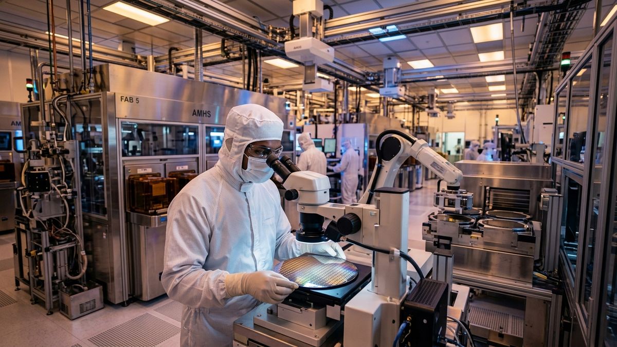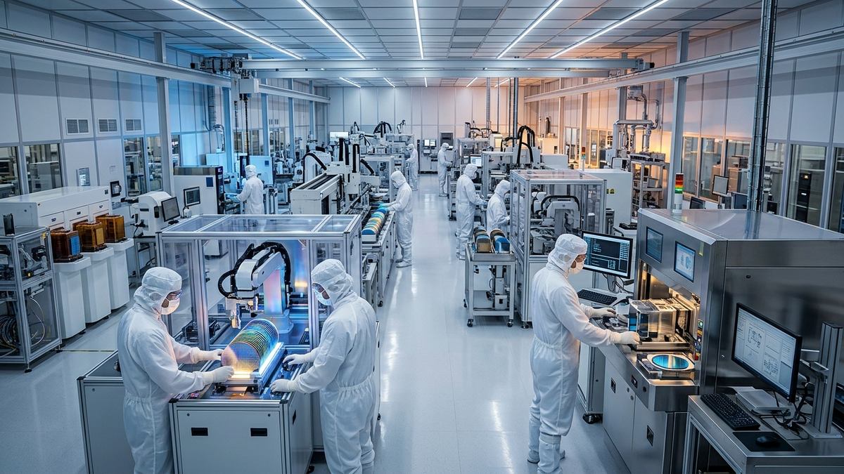
India's semiconductor manufacturing footprint reaches 12 approved projects across Gujarat, Assam, Odisha, UP, Andhra Pradesh, and Punjab under the India Semiconductor Mission.
Executive Key Takeaways
- The India Semiconductor Mission (ISM) has approved 12 semiconductor manufacturing projects with cumulative investments exceeding ₹1.64 lakh crore.
- Projects are distributed across six states: Gujarat, Assam, Odisha, Uttar Pradesh, Andhra Pradesh, and Punjab.
- Facilities encompass commercial silicon foundries, advanced packaging (ATMP/OSAT), compound semiconductor fabrication, and 3D glass integration.
India's multi-decade pursuit of semiconductor sovereignty has achieved a decisive operational milestone, with the India Semiconductor Mission (ISM) formally approving 12 semiconductor manufacturing and packaging projects representing a cumulative capital investment exceeding ₹1.64 lakh crore (approximately $19.8 billion). Far from remaining concentrated in a single industrial pocket, the approved silicon foundries, assembly and testing units, and compound semiconductor fabs are distributed across six Indian states: Gujarat, Assam, Odisha, Uttar Pradesh, Andhra Pradesh, and Punjab.
This geographic diversification establishes a resilient, decentralized microelectronics corridor across India. By strategically distributing capital-intensive fabs, outsourced semiconductor assembly and test (OSAT) facilities, and specialized compound semiconductor lines across varied geographies, India is protecting its emerging silicon supply chain against localized environmental disruptions while catalyzing high-tech industrialization across the nation.
The Six-State Silicon Matrix: Comprehensive Project Breakdown
The table below provides an exhaustive mapping of the approved semiconductor manufacturing projects across India's six silicon states:
| State | Primary Project / Enterprise | Technology Scope | Strategic Significance |
|---|---|---|---|
| Gujarat | Tata Electronics & PSMC (Dholera) | Commercial Silicon Wafer Fab (28nm, 55nm, 91nm) | India's First Commercial Mega-Fab Foundry |
| Gujarat | Micron Technology (Sanand) | DRAM & NAND Memory ATMP Packaging | Tier-1 Global Memory Assembly & Test |
| Gujarat | CG Power, Renesas & STARS (Sanand) | Legacy & Automotive OSAT Packaging | Industrial & Power Semiconductor Integration |
| Gujarat | Kaynes Semicon & Suchi Semicon | Specialized Optical & Multi-Chip OSAT | Smart Metering and Consumer Electronics |
| Assam | Tata Semiconductor Assembly & Test (TSAT) | High-Volume Semiconductor Assembly (Jagiroad) | Historic Deep-Tech Anchor for Northeast India |
| Odisha | SiCSem & 3D Glass Solutions | Silicon Carbide (SiC) Fab & 3D Advanced Packaging | Wide-Bandgap Power Chips for EVs & Rail |
| Uttar Pradesh | HCL & Foxconn Joint Venture | Advanced Display & Mobility OSAT (Jewar) | Proximity to Northern Consumer Electronics Belt |
| Andhra Pradesh | Advanced System in Package (ASIP) | High-Density System-in-Package Modules | Multi-Die Packaging for Communications |
| Punjab | CDIL (Continental Device India) | Silicon Power Transistors & Diodes (Mohali) | High-Reliability Discrete Power Semiconductors |
Gujarat and Assam: The Heavyweight Manufacturing Anchors
Gujarat has established itself as India's primary foundry and memory packaging capital. The Tata Electronics fab at Dholera, developed in partnership with Taiwan's Powerchip Semiconductor Manufacturing Corporation (PSMC) with an outlay of ₹91,000 crore, represents India's crown jewel. Spanning 28nm, 55nm, and 91nm process nodes, Dholera will produce chips for automotive engine control units, industrial automation, telecommunications gear, and consumer appliances. In Sanand, Micron Technology's $2.75 billion facility is preparing to deliver its first packaged memory modules, supported by joint ventures involving Renesas Electronics and CG Power.
Equally transformative is the Tata Semiconductor Assembly and Test (TSAT) facility in Jagiroad, Assam. Representing an investment of ₹27,000 crore and projected to produce 48 million chips daily, the facility marks the most significant high-tech industrial investment in the history of Northeast India, proving that semiconductor manufacturing can thrive far beyond traditional industrial zones.
Odisha, UP, Andhra, and Punjab: Specialized and Compound Silicon
While Gujarat and Assam anchor high-volume silicon and memory, other states have targeted specialized, high-margin microelectronics niches:
- Odisha's Silicon Carbide Prowess: In Bhubaneswar, SiCSem is constructing an indigenous silicon carbide (SiC) compound fab. SiC chips operate at vastly higher temperatures, voltages, and switching frequencies than standard silicon, making them indispensable for electric vehicle inverters, high-speed rail, and renewable energy substations. Concurrently, 3D Glass Solutions is establishing high-density glass substrate packaging for high-frequency RF applications.
- Uttar Pradesh's Electronics Synergy: In Jewar, adjacent to the upcoming international airport, the HCL–Foxconn joint venture will package chips for mobile devices and automotive mobility, feeding the massive electronics manufacturing clusters of Noida and Greater Noida.
- Punjab's Discrete Legacy: In Mohali, CDIL continues to expand its surface-mount semiconductor lines, producing aerospace-qualified discrete power devices that supply defense programs and space missions.
"A semiconductor fab cannot function in isolation; it requires an entire archipelago of chemical suppliers, ultra-pure gas providers, precision optics, and packaging hubs,"noted semiconductor industry analysts. "Spreading these 12 facilities across six states ensures that India's microelectronics infrastructure is robust, diversified, and embedded in local economic ecosystems."
Synergies with Domestic Deep-Tech Hardware
The nationwide expansion of semiconductor fabrication directly feeds India's rising deep-tech ventures. Domestic innovators such as SpectraGaze Systems developing spaceborne infrared sensors and Tonbo Imaging fabricating computational military optics will soon be able to package and fabricate sensors domestically rather than relying on overseas foundries.
With 12 approved projects steadily breaking ground and advancing cleanroom qualification, India's six semiconductor states are establishing the industrial foundation for a self-sustaining $100 billion domestic electronics manufacturing economy by the decade's end.
Frequently Asked Questions
What is the total committed investment and scope of approved projects under the India Semiconductor Mission?
The India Semiconductor Mission has approved 12 manufacturing and packaging projects representing a cumulative investment of more than ₹1.64 lakh crore (nearly $20 billion), backed by central and state fiscal incentives.
Which six Indian states currently host approved semiconductor manufacturing projects?
The approved projects span Gujarat (Dholera and Sanand), Assam (Jagiroad), Odisha (Bhubaneswar), Uttar Pradesh (Jewar/Greater Noida), Andhra Pradesh, and Punjab (Mohali).
What are the flagship projects leading India's commercial semiconductor push?
Flagship projects include Tata Electronics' commercial wafer fabrication plant in Dholera (in partnership with Taiwan's PSMC), Micron Technology's DRAM/NAND ATMP facility in Sanand, and Tata's massive packaging facility in Jagiroad, Assam.
Why is spreading semiconductor facilities across multiple states strategically advantageous?
Distributing fabs, OSAT units, and compound semiconductor plants across six states prevents geographic single-point-of-failure risks, utilizes diverse regional water and power resources, and spurs pan-India high-tech employment.
Primary Sources & Official References
- India Semiconductor Mission (ISM) & Digital India Corporation: Approved Projects Status Report
- Ministry of Electronics and Information Technology (MeitY): Gazette Notifications on Modified Semicon India Programme
- Tata Electronics Private Limited & Micron Technology: Construction and Qualification Timelines
- SEMI (Semiconductor Equipment and Materials International): Global Fab Investment and Supply Chain Benchmark