India's semiconductor push reaches physical reality as commercial fabs in Dholera, multi-billion-dollar OSAT units in Sanand, and RISC-V design incentives hit critical milestones.
Executive Key Takeaways
- India's semiconductor push reaches physical reality as commercial fabs in Dholera, multi-billion-dollar OSAT units in Sanand, and RISC-V design incentives hit critical milestones.
- Semiconductor fabrication is the most capital-intensive, technologically unforgiving manufacturing discipline on Earth, noted Dr. V. K. Saraswat, Member of NITI Aayog. By coupling 50% central fiscal support on project costs with matching state government incentives, India has eliminated the capital disadvantage that previously stymied domestic efforts. The operationalization of Dholera and Sanand guarantees that Indian industry will have sovereign access to foundational silicon.
- Key Benchmark: **Tata Electronics & PSMC** — Commercial Silicon Fab
NEW DELHI & GANDHINAGAR — India's ambitious industrial blueprint to establish a self-reliant domestic semiconductor ecosystem, powered by the central government's dedicated ₹13 Billion+ ($10B+ / ISM Phase 1 and 2) capital expenditure outlay, is achieving decisive physical and operational milestones. Construction activity is surging across flagship sites, led by Tata Electronics' commercial semiconductor fabrication plant in Dholera, Gujarat, in technical partnership with Taiwan's Powerchip Semiconductor Manufacturing Corporation (PSMC). Concurrently, multi-billion-dollar Outsourced Semiconductor Assembly and Test (OSAT) and ATMP facilities are advancing rapidly in Sanand and Assam, while the national Design Linked Incentive (DLI) scheme is funding dozens of domestic fabless startups designing custom RISC-V silicon. India is systematically dismantling its total reliance on foreign chip imports and carving out a strategic position in the global microelectronics supply chain.
This industrial momentum arrives as sovereign nations race to secure supply resilience against geopolitical vulnerabilities. Supported by specialized investment vehicles such as Piper Serica's ₹180–220 Crore Deep-Tech Bharat Tech Fund Deployments and foundational government execution frameworks detailed in India Semiconductor Mission 2.0, the country is proving that long-term industrial policy can translate into operational silicon foundries.
Foundation of Commercial Fabs and Advanced OSAT Facilities
The physical centerpieces of the India Semiconductor Mission (ISM) represent a sophisticated balance between high-volume commercial foundries and fast-to-market advanced packaging facilities:
1. The Tata-PSMC Dholera Mega-Fab
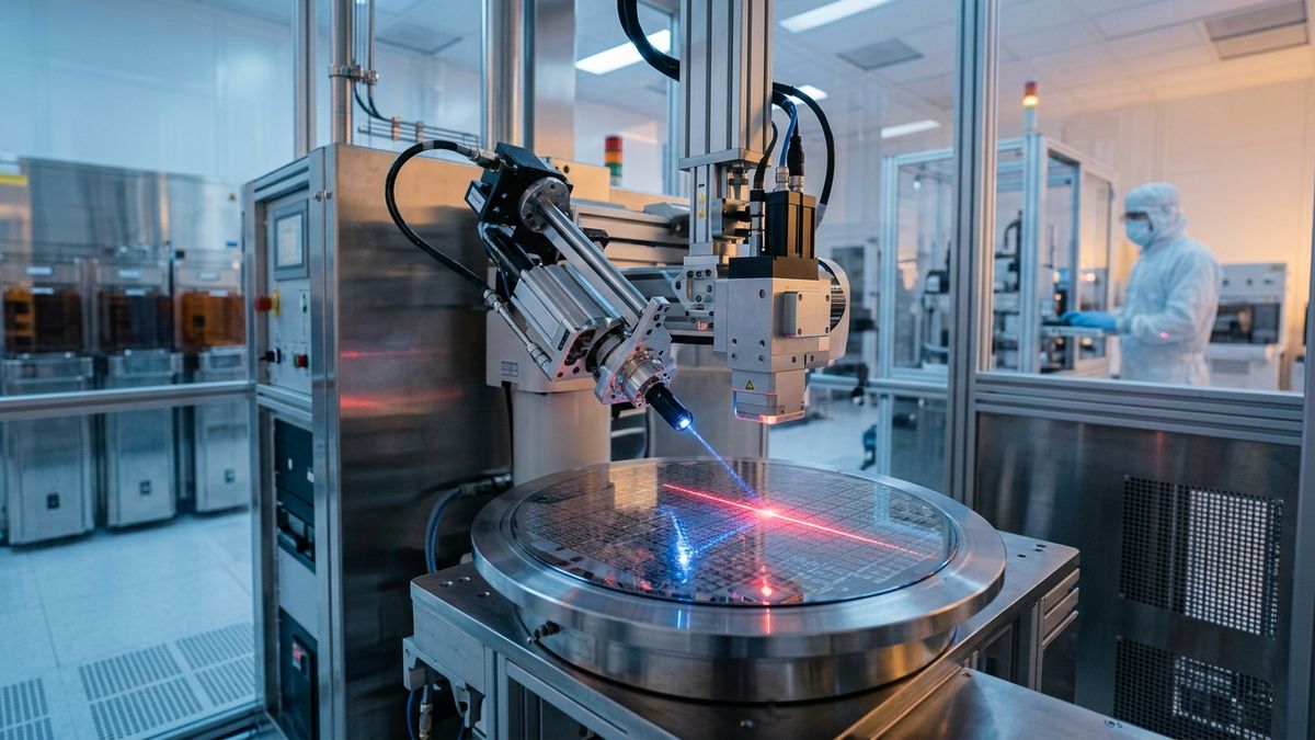
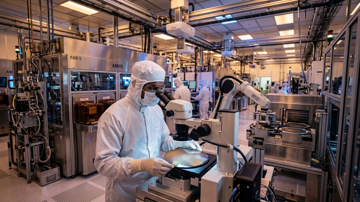
Located within the Dholera Special Investment Region (SIR) in Gujarat, Tata Electronics' ₹91,000 crore ($11 billion) mega-foundry marks India's premier commercial front-end fabrication milestone. Partnering with Taiwan's PSMC, the fab is engineered for an operational capacity of up to 50,000 wafer starts per month (WSPM). Fabricating silicon across mature and legacy nodes—specifically 28-nanometer, 40-nanometer, 55-nanometer, and 90-nanometer processes—the facility directly targets foundational automotive microcontrollers, power management integrated circuits (PMICs), high-reliability telecommunications switches, and defense electronics.
2. The Sanand Semiconductor Hub: Micron & CG Power
In Sanand, Gujarat, Micron Technology's $2.75 billion ATMP facility has completed structural build-out, preparing to package advanced NAND flash memory and DRAM modules for domestic consumer electronics and global server exports. Simultaneously, the joint venture between CG Power, Renesas Electronics (Japan), and Stars Microelectronics (Thailand) is establishing an adjacent ₹7,600 crore OSAT unit focused on specialized automotive and industrial motor controllers.
3. Northeast Expansion: Tata's Morigaon Assembly Campus
Expanding the semiconductor footprint beyond western industrial corridors, Tata Electronics is constructing a massive ₹27,000 crore advanced packaging unit in Morigaon, Assam. Engineered for advanced wire-bond, flip-chip, and system-in-package (SiP) modules, the facility is slated to produce over 48 million semiconductor packages per day, positioning Northeast India as an essential electronics node for global original design manufacturers (ODMs).
"Semiconductor fabrication is the most capital-intensive, technologically unforgiving manufacturing discipline on Earth,"noted Dr. V. K. Saraswat, Member of NITI Aayog. "By coupling 50% central fiscal support on project costs with matching state government incentives, India has eliminated the capital disadvantage that previously stymied domestic efforts. The operationalization of Dholera and Sanand guarantees that Indian industry will have sovereign access to foundational silicon."
The Fabless Revolution: RISC-V Silicon and DLI Capital
While heavy fabrication plants secure hardware manufacturing sovereignty, India's long-term competitive edge lies in chip design. India currently houses over 20% of the world's semiconductor design engineers working in multinational GCCs (Global Capability Centers); the ISM's Design Linked Incentive (DLI) scheme seeks to redirect that intellectual horsepower toward domestic intellectual property (IP) creation.
By leveraging open-standard RISC-V processor architectures, Indian fabless ventures are bypassing expensive proprietary licensing fees from ARM and x86 architectures:
- Mindgrove Technologies: Spun out of the IIT Madras SHAKTI processor program, Mindgrove has successfully taped out the Secure IoT microprocessor, engineered for connected consumer appliances, smart utility meters, and edge computing at a fraction of imported silicon costs.
- InCore Semiconductors: Delivering configurable RISC-V processor cores tailored for automotive telematics, mission-critical industrial controllers, and defense communications.
- Metrology and Inspection Startups: Developing indigenous wafer-level quality assurance equipment, highlighted by companies like Makr Microsystems Raising ₹10.2 Crore for Semiconductor Metrology and Defect Detection.
Comprehensive Overview: Major Indian Semiconductor Initiatives
The comprehensive table below outlines the core projects, investment outlays, technology nodes, and commercial horizons approved under the India Semiconductor Mission:
| Entity / Consortium | Project Type | Geographic Location | Capex Outlay | Target Technology / Nodes | Projected Output / Application |
|---|---|---|---|---|---|
| Tata Electronics & PSMC | Commercial Silicon Fab | Dholera, Gujarat | ₹91,000 Crore ($11.0B) | 28nm, 40nm, 55nm, 90nm Logic | 50,000 WSPM; Automotive, Power, Telecom |
| Micron Technology | ATMP / Packaging | Sanand, Gujarat | ₹22,500 Crore ($2.75B) | Advanced DRAM & NAND Flash | Server Memory, Mobile Storage, Solid-State Drives |
| Tata Electronics (Assam) | Advanced OSAT / SiP | Morigaon, Assam | ₹27,000 Crore ($3.25B) | Flip-Chip, Wire-Bond, SiP | 48 Million Packages/Day; Global Consumer Electronics |
| CG Power, Renesas & Stars | Specialized OSAT | Sanand, Gujarat | ₹7,600 Crore ($910M) | Legacy & Specialized Silicon | 15 Million Chips/Day; Automotive Power & IoT |
| Kaynes Semicon | OSAT / Module Assembly | Sanand, Gujarat | ₹3,300 Crore ($400M) | High-Density System Modules | 6 Million Chips/Day; Industrial Automation & EV |
Overcoming Equipment, Pure-Gas, and Cleanroom Bottlenecks
A semiconductor fab cannot function in isolation; it requires an intricate, hypersensitive supporting industrial ecosystem. A single 28nm fabrication run consumes millions of liters of ultra-pure water (UPW), uninterrupted megawatts of ultra-clean electricity, and specialized gases including silane, phosphine, and ultra-high-purity nitrogen.
To insulate Dholera and Sanand from supply disruptions, the central and state governments have implemented dedicated infrastructure corridors:
1. Dedicated Water Desalination Pipelines: Guaranteeing continuous supplies of industrial-grade water with parts-per-trillion purity tolerances.
2. Tri-Redundant Power Substations: Preventing voltage fluctuations that could ruin weeks-long wafer diffusion runs.
3. Specialty Chemical & Gas Hubs: Partnering with global chemical leaders (such as Linde and Air Liquide) to manufacture high-purity process gases domestically.
4. Deeptech Incubation & Commercialization: Leveraging platforms such as LTTS's Platform to Help Deeptech Startups Scale to foster tier-2 and tier-3 domestic equipment vendors.
The Human Capital Pipeline: Training 85,000 Chip Engineers
A foundational pillar of the India Semiconductor Mission is the Chips to Startup (C2S) initiative, designed to train over 85,000 industry-ready B.Tech, M.Tech, and Ph.D. engineers across VLSI design, semiconductor chemistry, cleanroom maintenance, and metrology over a five-year horizon.
Through partnerships with global Electronic Design Automation (EDA) titans including Synopsys, Cadence Design Systems, and Siemens EDA, India has deployed commercial-grade chip simulation software across more than 300 universities and engineering colleges. Undergraduates and graduate researchers are now designing, validating, and submitting custom silicon tape-outs before graduation, eliminating the multi-year training latency that previously burdened corporate employers.
Geopolitical Tailwinds and the Future of Sovereign Microelectronics
Global electronics manufacturers—seeking to hedge against geopolitical tensions in East Asia and catastrophic supply chain choke-points—regard India as a viable alternative for semiconductor sourcing and advanced packaging.
With automotive giants transitioning toward electric powertrains requiring thousands of chips per vehicle, domestic telecom operators expanding 5G and satellite networks, and sovereign defense programs mandating encrypted, tamper-proof hardware, the economic justification for India's ₹13 Billion+ semiconductor mission has never been more compelling. As fabs and packaging facilities complete tool hook-up and commence pilot wafer runs, India is asserting its place as an indispensable anchor of the global silicon economy.