India Targets 200 Chip-Design Companies Under ISM 2.0 as Over 105 Startups Access Enterprise EDA Tools
By Karthik Ramaswamy | Published October 1, 2026 | 8 min read
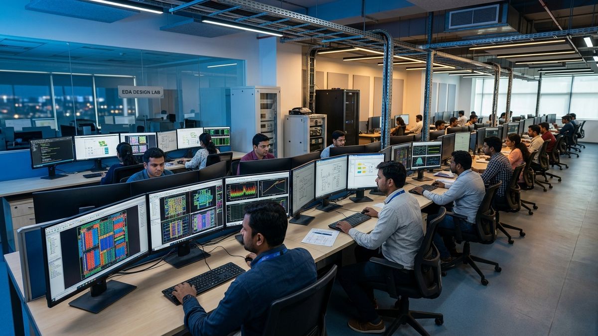
India expands India Semiconductor Mission 2.0 targeting 200 domestic fabless chipmakers, with over 105 startups already empowered by subsidized enterprise EDA design suites.
The Ministry of Electronics and Information Technology (MeitY) has officially expanded the India Semiconductor Mission (ISM 2.0), setting an ambitious target to incubate and scale 200 domestic chip-design companies across the country. As a foundational pillar of this initiative, more than 105 fabless semiconductor startups have already received centralized access to state-of-the-art Electronic Design Automation (EDA) software suites through the government's ChipIN Centre, dramatically reducing the capital barriers to silicon prototyping.
While the initial phase of the semiconductor mission laid the groundwork for commercial fabrication foundries and outsourced semiconductor assembly and test (OSAT) facilities, ISM 2.0 pivots aggressively toward high-margin intellectual property (IP). India already contributes over 20% of the world's semiconductor design workforce, but the vast majority have historically worked inside multinational design centres. ISM 2.0 aims to transform this deep engineering talent into domestic fabless founders.
This fabless silicon boom complements major funding milestones in physical computing, exemplified by recent breakthroughs like SiMa.ai's $150M physical AI silicon round, highlighting the massive global appetite for specialized edge microprocessors.
Dismantling the Capital Barrier: The ChipIN Centre and EDA Democratization
Historically, launching a fabless semiconductor startup required millions of dollars in upfront capital simply to license enterprise EDA tools from global leaders like Synopsys, Cadence Design Systems, and Siemens EDA. Without these specialized computer-aided design platforms, designing complex integrated circuits, simulating thermal kinetics, and verifying physical timing closures is impossible.
The government-established ChipIN Centre at C-DAC has completely altered this equation:
- Centralized Cloud Access: Startups and academic researchers log into high-performance compute clusters hosting verified licenses of industry-standard EDA tools, eliminating prohibitive on-premise software procurement costs.
- Process Design Kit (PDK) Access: Pre-integrated access to foundry PDKs from premier global foundries (including TSMC, GlobalFoundries, and SCL Mohali), enabling startups to design directly for target process nodes ranging from 180nm to 7nm.
- Design Verification and Emulation: Shared hardware emulation platforms and FPGA prototyping racks that allow engineers to test silicon logic at speed before committing to multi-million-dollar photomask production.
"India has the engineering minds that design the world's most intricate microprocessors,"stated senior officials at MeitY. "Under ISM 2.0, our mission is to ensure that no Indian chip designer is stopped by the high cost of EDA software. By providing world-class tools and tape-out subsidies, we are building 200 sovereign semiconductor powerhouses."
ISM 2.0 Support Architecture: Strategic Components Matrix
The table below outlines the core components, operational subsidies, and milestone targets established under India Semiconductor Mission 2.0:
| Policy Component | Operational Agency | Financial Incentive / Subsidy Provision | Strategic Target (ISM 2.0) |
|---|---|---|---|
| Design Linked Incentive (DLI) | MeitY / C-DAC | Up to 50% reimbursement of R&D expenses (up to Rs 15 Cr) | Scale domestic fabless startups to 200 ventures |
| ChipIN EDA Software Cloud | C-DAC Pune | 100% subsidized cloud access to Cadence, Synopsys, Siemens | Empower 120+ startups & 150+ academic universities |
| Tape-Out Prototyping Grant | ISM Directorate | Subsidized multi-project wafer (MPW) shuttle runs | 50+ successful silicon tape-outs across domestic fabs |
| Deployment-Linked Incentive | Ministry of Finance | 4% to 6% incentive on net domestic product sales over 5 yrs | Drive commercial adoption in smart meters & automotive |
| Semiconductor Talent Mandate | AICTE / NIELIT | VLSI curriculum integration across 300+ engineering colleges | Train 85,000 industry-ready chip design engineers |
High-Growth Silicon Verticals: Where Indian Startups Are Winning
Rather than attempting to compete immediately in ultra-advanced 3nm smartphone processors, Indian fabless startups are targeting high-growth, high-margin specialized verticals:
- Power Management ICs (PMICs): High-efficiency voltage regulator chips optimized for electric two-wheelers, solar inverters, and battery management systems.
- RISC-V Edge Microcontrollers: Open-standard compute cores for industrial smart metering, IoT sensors, and consumer appliances, eliminating foreign proprietary architecture royalties.
- Physical AI and Vision Processors: Custom neural processing units (NPUs) built for edge cameras, robotics defect inspection, and autonomous navigation.
- RF and Telecom Silicon: Gallium Nitride (GaN) and CMOS radio-frequency amplifiers tailored for 5G base stations and defense communication transceivers.
Nurturing Talent and Building Long-Term IP Value
The success of ISM 2.0 relies on close coordination between government policy, venture capital, and engineering academia. Initiatives like industry-academia deeptech hackathons are bridging the transition from university theory to production-grade physical layout engineering.
As global supply chains aggressively seek geographical diversification, India's deliberate strategy to cultivate 200 fabless chip designers positions the country not just as a manufacturing destination, but as an indispensable creator of core semiconductor intellectual property for the twenty-first century.
Frequently Asked Questions
What is India Semiconductor Mission (ISM) 2.0 and how does it prioritize chip design?
ISM 2.0 is the second phase of India's national semiconductor policy. Unlike ISM 1.0 which focused heavily on large fabrication and packaging units, ISM 2.0 aggressively prioritizes indigenous fabless design, targeting 200 domestic chip design startups with financial incentives and EDA tooling access.
What is the ChipIN Centre and what EDA tools does it provide to startups?
The ChipIN Centre, hosted at C-DAC, is a centralized national cloud facility providing verified semiconductor startups and academic institutes with subsidized, turnkey access to industry-standard EDA tools from Synopsys, Cadence, and Siemens EDA.
How does the Design Linked Incentive (DLI) scheme help fabless chip startups financially?
The DLI scheme offers financial reimbursement of up to 50% of eligible design and development expenditure (capped at Rs 15 crore per startup) alongside deployment-linked incentives of 4% to 6% on net sales turnover over five years.
What semiconductor product categories are Indian chip-design startups focusing on?
Startups are designing specialized microchips across power management integrated circuits (PMICs), RISC-V edge microcontrollers, Physical AI accelerators, automotive sensors, and 5G telecom signal processors.
Primary Sources & Official References
- Ministry of Electronics and Information Technology (MeitY): ISM 2.0 Policy Framework
- India Semiconductor Mission (ISM): Design Linked Incentive (DLI) Scheme Directorate
- Centre for Development of Advanced Computing (C-DAC): ChipIN Centre Operational Report
- India Electronics and Semiconductor Association (IESA): Semiconductor Talent & Design Ecosystem 2026