Fujifilm Expands India Semiconductor Ambitions Through Strategic Materials Partnership With Tata Electronics
By Rohan Varma | Published September 20, 2026 | 8 min read
Japanese chemical and imaging giant Fujifilm enters a strategic semiconductor materials partnership with Tata Electronics to supply ultra-pure process chemicals for India's upcoming wafer fabs.
In a landmark move that solidifies the upstream foundations of India's semiconductor manufacturing ecosystem, Japanese multinational chemical and technology conglomerate Fujifilm has announced a strategic semiconductor materials partnership with Tata Electronics. The alliance secures the direct supply and progressive domestic localization of ultra-high-purity electronic process chemicals, photolithography formulations, and advanced packaging materials essential for Tata Electronics' upcoming commercial wafer fab in Dholera, Gujarat, and packaging complex in Jagiroad, Assam.
As global semiconductor manufacturers look to de-risk geographic dependencies, the partnership represents a decisive validation of India's semiconductor corridor by one of Japan's premier electronic materials manufacturers. The collaboration ensures that India's mega-fabs will have direct, uninterrupted access to certified Tier-1 specialty chemicals, mitigating one of the most complex logistical bottlenecks in semiconductor fabrication.
The Invisible Foundation: Ultra-Pure Electronic Specialty Chemicals
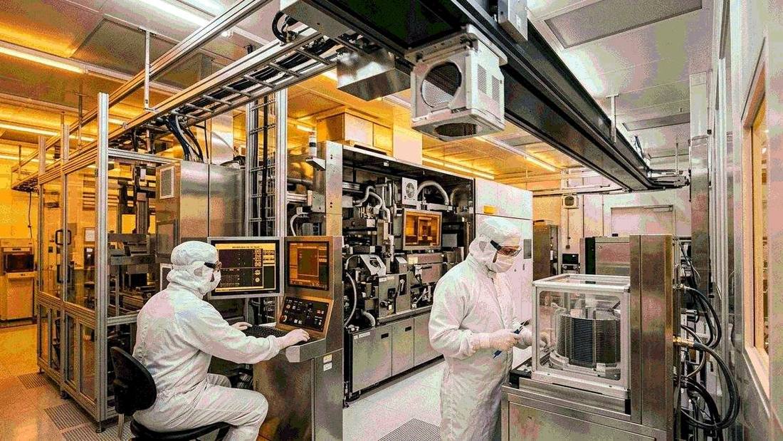
While public attention in the semiconductor industry is often captivated by multi-billion-dollar extreme ultraviolet (EUV) lithography scanners and robotic cleanrooms, a wafer fab cannot produce a single functional microchip without an uninterrupted stream of ultra-high-purity chemicals:
- Parts-Per-Trillion (PPT) Purity Standards: Semiconductor chemical grades require purity levels where foreign contaminants cannot exceed a few parts per trillion. A single microscopic metal ion or dust grain in a photoresist batch can bridge nanometer-spaced transistor gates, causing electrical short circuits across entire silicon wafers.
- Strict Shelf-Life Limitations: Advanced photolithography chemicals and specialty developer fluids degrade rapidly over time and must be transported under cryogenic, temperature-controlled conditions. Relying exclusively on trans-continental air freight introduces unacceptable operational and financial vulnerabilities.
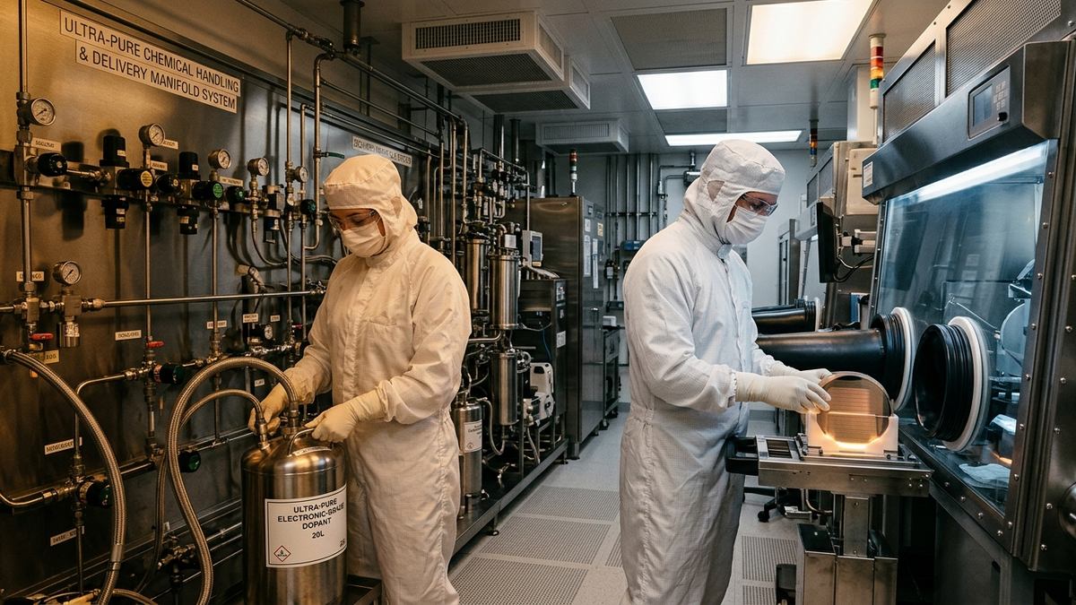
- Hazardous Materials Compliance: Specialty etching acids and toxic carrier solvents require specialized double-walled stainless steel storage containers and certified automated chemical distribution systems (CDS) directly integrated into the sub-fab level.
By partnering with Fujifilm, Tata Electronics establishes an integrated materials supply chain that combines Japanese chemical synthesis precision with localized cleanroom distribution infrastructure.
"A semiconductor fab is fundamentally a massive precision chemical processing plant that happens to output microchips,"remarked semiconductor materials specialists. "Fujifilm’s strategic commitment to Tata Electronics proves that global Tier-1 suppliers view India’s semiconductor mission not as a temporary pilot, but as a permanent manufacturing hub."
This materials pact builds directly upon the milestone announcements witnessed at SEMICON India 2026 where 56 strategic MoUs united 52 nations and aligns with Micron scaling up Sanand's commercial memory assembly operations.
Scope of the Strategic Partnership
The collaboration between Fujifilm and Tata Electronics covers three foundational areas across both front-end wafer processing and back-end advanced packaging:
| Material Category | Application in Fab / ATMP | Technical Specifications | Strategic Supply Benefit |
|---|---|---|---|
| Photolithography Materials | Wafer patterning in Dholera Fab | Advanced DUV photoresists, antireflective coatings | Precise sub-micron feature resolution for 28nm/40nm nodes |
| CMP Slurries & Cleaners | Chemical Mechanical Planarization | High-selectivity silica and ceria abrasive slurries | Atomically flat wafer planarization across dielectric layers |
| Advanced Packaging Adhesives | 2.5D/3D Packaging in Jagiroad | Low-stress epoxy underfills, polyimide dielectric films | Prevents thermal warpage in high-power automotive chips |
| Ultra-Pure Process Solvents | Wafer cleaning & wet chemical benches | PPT-grade isopropyl alcohol (IPA), high-purity strippers | Zero-defect surface preparation post-plasma etching |
Localized Technical Service Laboratories and Testing
Beyond direct chemical procurement, the partnership includes the establishment of a dedicated Fujifilm Electronic Materials Technical Service Centre in Gujarat. The facility will house high-precision gas chromatography, mass spectrometry, and automated particle counters to conduct real-time chemical quality assurance on-site.
Engineers from Fujifilm will work side-by-side with Tata Electronics' cleanroom specialists to optimize chemical dispense rates, reduce chemical waste through advanced reclamation systems, and tailor specific chemical mechanical planarization (CMP) formulations to match the electrical performance profiles demanded by global automotive and industrial clients.
Deepening the Indo-Japanese Semiconductor Corridor
The Fujifilm-Tata Electronics agreement is a cornerstone achievement of the bilateral semiconductor partnership established between India's Ministry of Electronics and IT (MeitY) and Japan's Ministry of Economy, Trade and Industry (METI). Japan controls more than 50% of the worldwide market for critical semiconductor materials and specialty chemicals, making Japanese corporate participation indispensable to the success of the India Semiconductor Mission (ISM).
With Fujifilm establishing long-term operations in India, industry analysts anticipate that other Japanese semiconductor supply-chain anchors—including silicon wafer manufacturers, quartz glass suppliers, and vacuum pump specialists—will accelerate their own Indian localization strategies.
Accelerating toward 2027 Commercial Pilot Production
With construction at Tata Electronics' Dholera facility progressing rapidly and cleanroom structural shells taking shape, the integration of certified chemical delivery infrastructure ensures that pilot qualification runs scheduled for 2027 will proceed without supply-chain delays.
Through this strategic alliance, India is not merely constructing wafer fabrication plants—it is weaving a robust, comprehensive, and resilient semiconductor ecosystem capable of sustaining advanced microelectronics manufacturing for generations to come.
Frequently Asked Questions
What is the focus of the partnership between Fujifilm and Tata Electronics?
The strategic partnership focuses on establishing a resilient supply chain of ultra-pure semiconductor electronic chemicals, advanced photoresists, chemical mechanical planarization (CMP) slurries, and specialized packaging materials for Tata Electronics' facilities in Gujarat and Assam.
Why are electronic chemicals critical for semiconductor wafer fabrication?
Modern semiconductor lithography and etching require parts-per-trillion (PPT) ultra-pure chemicals. Even microscopic chemical impurities can destroy nanometer-scale transistor gates and ruin entire silicon wafer batches.
Where are Tata Electronics' semiconductor facilities located?
Tata Electronics is constructing a ₹91,000 crore commercial wafer fabrication facility in Dholera, Gujarat (in partnership with Taiwan's PSMC), and a ₹27,000 crore greenfield semiconductor packaging facility in Jagiroad, Assam.
How does Fujifilm's participation benefit India's broader chip ecosystem?
Fujifilm's entry establishes local technical service laboratories, trains chemical engineers in cleanroom handling standards, and encourages other Tier-1 Japanese materials suppliers to invest in Indian semiconductor corridors.
Primary Sources & Official References
- Fujifilm Corporation Electronic Materials Division: Official Announcement of Strategic Semiconductor Partnership: Corporate disclosure on global materials expansion.
- Tata Electronics Private Limited: Press Communiqué on Upstream Supply Chain Alliances: Official statement on Dholera and Jagiroad supplier ecosystem.
- India Semiconductor Mission (ISM): Comprehensive Chemical & Materials Infrastructure Guidelines: Regulatory frameworks governing electronic specialty chemicals.
- Japan External Trade Organization (JETRO): Bilateral Japan-India Semiconductor Supply Chain Report: Economic telemetry on Japanese high-tech investments in India.