Micron to Scale Up India Chip Operations: Sanand Assembly & Test Facility Targets Massive Capacity Expansion in 2027
By Sanjay Patel | Published September 18, 2026 | 8 min read
Micron prepares to aggressively scale assembly and testing at its $2.75B Sanand facility next year, expanding domestic memory packaging and global semiconductor exports.
Micron Technology is preparing to aggressively scale assembly and testing operations at its landmark semiconductor packaging facility in Sanand, Gujarat, starting early next year as global memory chip production accelerates. Backed by the India Semiconductor Mission (ISM) with a combined central and state government incentive framework representing a total project investment of $2.75 billion, the facility's forthcoming operational ramp-up marks a transformative milestone. The expansion will transition India from an established leader in fabless chip design into an active physical hub for commercial semiconductor manufacturing and global high-volume export distribution.
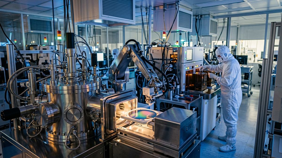
The Sanand complex, which began pilot line trials and initial component testing in 2025, is now finalizing its ultra-cleanroom infrastructure, automated material handling systems, and advanced automated test equipment (ATE) suites. The upcoming phase will dramatically multiply high-speed packaging throughput for dynamic random-access memory (DRAM) and NAND flash solid-state storage products destined for automotive electronics, enterprise AI servers, smartphones, and industrial edge computing systems across Asia, Europe, and North America.
Phase-Wise Cleanroom Readiness and Scaling Trajectory
The scale-up plan centers on bringing the primary cleanroom of Phase 1 to full commercial utilization while expediting Phase 2 civil infrastructure. Advanced semiconductor assembly, testing, marking, and packaging (ATMP)—often termed Outsourced Semiconductor Assembly and Test (OSAT)—requires micro-environmental controls rivaling frontend wafer fabs.
Key operational milestones underpinning Micron's scale-up include:
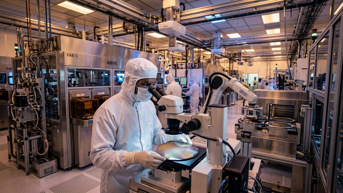
* Class 10,000 and Class 1,000 Cleanroom Activation: Deploying positive-pressure laminar airflow and HEPA filtration systems to eliminate airborne particulates across 500,000 square feet of dedicated cleanroom space.
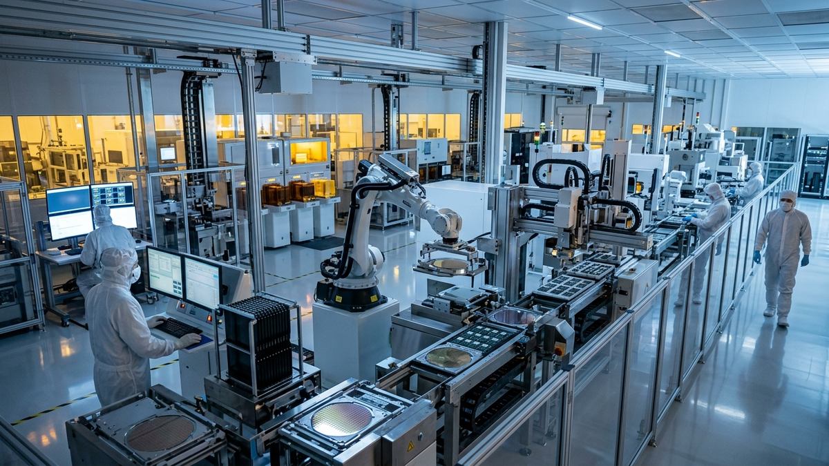
* Robotic Die-Attach and Wire-Bonding Lines: Integrating multi-axis robotic handlers that place dicing-sawed silicon wafers onto high-density multi-layer organic substrates with sub-micron precision.
* Automated Ball Grid Array (BGA) Packaging: Encapsulating sensitive silicon dies in high-reliability thermoset epoxy compounds engineered to withstand automotive temperature extremes (-40°C to +125°C).
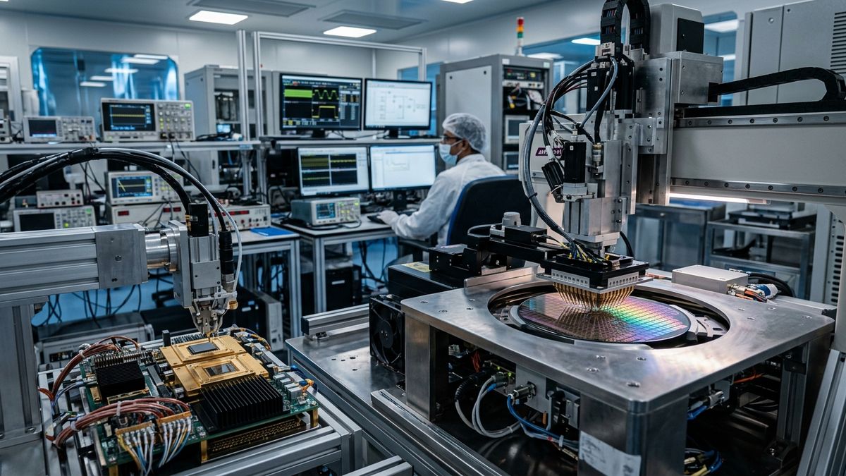
* High-Speed Automated Test Equipment (ATE): Running multi-parametric stress testing, thermal cycling, and functional signal-integrity verification to achieve automotive zero-defect standards (AEC-Q100).
"Our Sanand facility represents one of the most technologically advanced memory packaging plants in the world,"stated senior semiconductor operations executives familiar with the expansion. "Scaling high-volume assembly and testing next year is not merely an internal milestone for Micron; it validates India's industrial execution capability for precision microelectronics manufacturing at global scale."
Integrating into Global Semiconductor Supply Chains
Historically, raw silicon wafers fabricated in East Asian or North American foundries were shipped exclusively to packaging hubs in Taiwan, Malaysia, or mainland China. Micron's scale-up in Gujarat establishes a resilient alternative corridor in South Asia, insulating multinational OEMs from geopolitical bottlenecks and single-geography shipping vulnerabilities.
The facility will process advanced memory formats:
1. LPDDR5X Memory Modules: Designed for next-generation AI smartphones, edge devices, and automotive digital cockpits requiring ultra-low latency and multi-gigabit throughput.
2. Enterprise NVMe SSDs: Multi-terabyte solid-state storage blades built for hyperscale cloud data centres and GPU cluster environments.
3. UFS 4.0 Embedded Storage: High-density flash packaging for connected IoT controllers, consumer wearables, and autonomous vehicle telemetry units.
This commercial expansion reinforces earlier hardware supply chain developments, including Lam Research's ₹10,000 Cr investment in precision silicon component equipment and Teradyne's expansion of automated chip testing and validation in Bengaluru.
Operational Blueprint: Micron Sanand Facility Milestones
The table below provides a comprehensive structural breakdown of Micron's Sanand capital allocation, technical specifications, and production targets:
| Operational Dimension | Initial Pilot Phase (2025) | Commercial Scale-Up (2027 Target) | Long-Term Target (Phase 1 & 2) |
|---|---|---|---|
| Total Cumulative Capex | $825 Million | $1.80 Billion | $2.75 Billion |
| Cleanroom Area | 150,000 sq. ft. | 500,000 sq. ft. | 1,000,000+ sq. ft. |
| Primary Memory Products | Ball Grid Array DRAM | LPDDR5X & NVMe SSDs | Multi-Chip Architectures & HBM |
| Testing Architecture | Prototype Validation & ATE | High-Volume Parametric Stress | Full-Spectrum Burn-In & QA |
| Direct & Indirect Employment | 1,200 Engineers & Technicians | 5,000+ Technical Specialists | 20,000+ Ecosystem Jobs |
| Target Export Destinations | Regional Test Markets | APAC, EU & North America | 100% Integrated Global Hub |
Catalyst for the Broader Domestic Semiconductor Ecosystem
Micron's accelerated schedule is producing a powerful multiplier effect across India's microelectronics supplier base. Under the India Semiconductor Mission, high-purity chemical suppliers, specialty gas manufacturers (such as ultra-pure nitrogen, argon, and silane), leadframe suppliers, and precision testing labs are co-locating in the Sanand-Dholera industrial belt.
Furthermore, domestic chip verification and design ventures—such as VerifAIX's AI-driven silicon verification platform—are gaining domestic test partners, closing the historical gap between local fabless RTL designers and physical packaging test facilities.
Strategic Outlook for 2027 and Beyond
As Micron transitions from qualification runs to multi-million-unit monthly output, the facility will serve as the commercial anchor for subsequent mega-projects, including the Tata Electronics-PSMC commercial wafer fab in Dholera and the CG Power-Renesas OSAT plant in Sanand. By establishing institutional mastery over high-yield cleanroom logistics, hazardous material safety protocols, and uninterrupted power-water grid integration, India is solidifying its position on the global semiconductor roadmap.