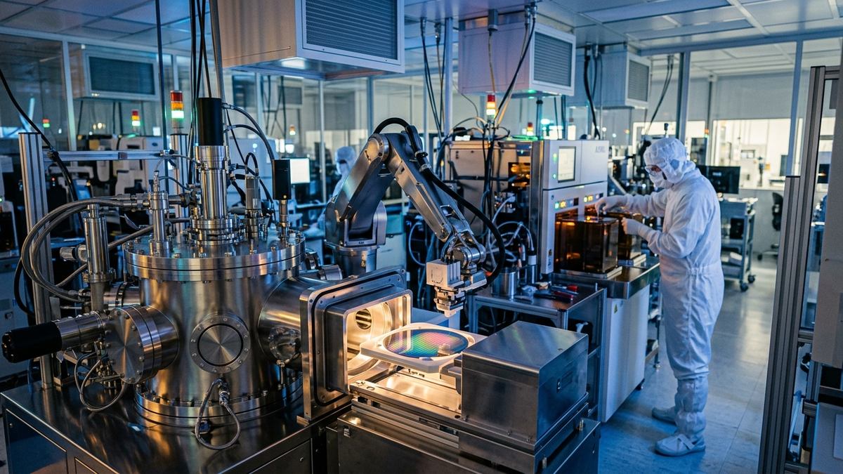
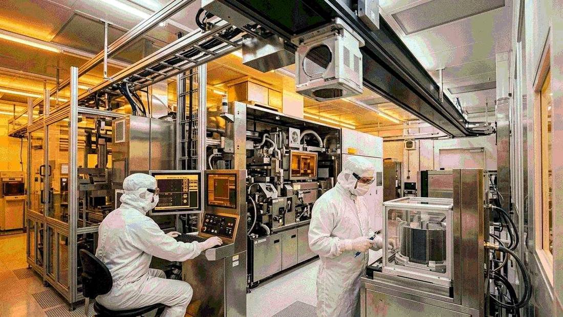
Tata Electronics Builds India’s Semiconductor Ecosystem Across Materials, Packaging, and Fab Equipment
By Sanjay Patel | Published September 22, 2026 | 9 min read
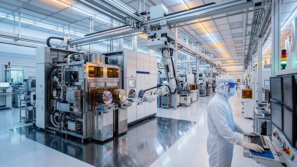
Tata Electronics is aggressively assembling an end-to-end semiconductor ecosystem, forging global alliances across fab tools, specialty gases, advanced OSAT packaging, and cleanroom talent.
Tata Electronics is aggressively accelerating global and domestic partnerships across capital equipment, specialty materials, advanced packaging, and cleanroom logistics, assembling India's first fully integrated commercial semiconductor value chain. Rather than treating its manufacturing sites as isolated industrial islands, the conglomerate is building an interdependent ecosystem capable of sustaining high-volume wafer fabrication and packaging on Indian soil.
The initiative centers around Tata Electronics' twin mega-projects: a ₹91,000 crore ($11 billion) commercial wafer fabrication facility in Dholera, Gujarat, developed in partnership with Taiwan's Powerchip Semiconductor Manufacturing Corporation (PSMC), and a ₹27,000 crore ($3.3 billion) greenfield semiconductor assembly, testing, and packaging (OSAT) complex in Jagiroad, Assam. As construction at both hubs advances ahead of scheduled 2027 pilot production, the group is methodically stitching together the complex upstream and downstream networks that make high-volume chip manufacturing economically viable.
The Multi-Layered Semiconductor Supply Chain Imperative
Modern semiconductor manufacturing is widely recognized as the most complex manufacturing endeavor in human history. A single commercial wafer fab requires thousands of specialized inputs: extreme-ultraviolet (EUV) and deep-ultraviolet (DUV) photolithography tools, high-purity silicon ingots, corrosive etching gases, copper sputtering targets, and sub-nanometer planarization slurries. Any disruption in this delicate supply chain can halt cleanroom operations, generating millions of dollars in idle fab losses per day.
Recognizing that semiconductor self-reliance cannot be achieved merely through building cleanroom shells, Tata Electronics has initiated formal supplier development programs across five core operational verticals:
- Capital Equipment & Tooling Maintenance: Establishing certified field-service centers and component staging warehouses with tier-1 toolmakers for lithography, chemical vapor deposition (CVD), plasma etch, and metrology inspection.
- Ultra-High-Purity Process Chemicals & Bulk Gases: Partnering with chemical giants to construct on-site nitrogen, argon, and hydrogen generation plants, as well as ultra-pure wet chemical delivery systems engineered to parts-per-trillion (PPT) purity thresholds.
- Advanced Packaging Substrates & Leadframes: Securing high-density organic interconnects, ball-grid array substrates, and gold/copper bonding wires for high-throughput packaging in Assam.
- Cleanroom Cold-Chain & Hazardous Logistics: Developing temperature-regulated, vibration-damped transportation corridors between international ports, regional airports, and fabrication hubs.
- Semiconductor Human Capital & Cleanroom Certification: Collaborating with national engineering institutes and global training academies to build a certified domestic operating workforce.
This strategic expansion builds upon major milestones, such as Fujifilm's strategic semiconductor materials partnership with Tata Electronics, and integrates closely with policy commitments finalized during SEMICON India 2026 which saw 56 strategic announcements.
"A modern semiconductor fab cannot operate as an isolated island of technology,"stated industry supply-chain strategists during recent investor briefings. "Without local supplier ecosystems, specialized gas lines, precision calibration workshops, and certified cleanroom technicians within a two-hour radius, sustaining 95%-plus fab yield rates is practically impossible. Tata Electronics is deliberately laying down the industrial railway tracks before the first train rolls out."
Upstream Alliances: Process Chemicals, Lithography, and Substrates
A major breakthrough in Tata Electronics' supply chain roadmap is the formal engagement of Japanese, European, and Taiwanese chemical suppliers. The manufacturing of 28nm and 40nm logic chips at Dholera demands electronic-grade hydrofluoric acid, sulfuric acid, photoresists, and CMP (Chemical Mechanical Planarization) slurries that cannot tolerate standard industrial impurities.
To eliminate international shipping lead times and insulate domestic production from geopolitical chokepoints, Tata Electronics is incentivizing specialty materials producers to establish formulation facilities inside the Dholera Special Investment Region (DSIR). In parallel, the company has entered long-term supply agreements for electronic specialty gases—including silane, phosphine, and sulfur hexafluoride—ensuring continuous pipelines directly into the cleanroom sub-fab basements.
Strategic Pillar Matrix: Tata Semiconductor Ecosystem Dimensions
The following structured matrix outlines the operational pillars, international alliances, and domestic milestones driving Tata Electronics' ecosystem expansion:
| Strategic Pillar | Focus Domain & Capability | Target Facility | Key Operational Benchmark |
|---|---|---|---|
| Wafer Fabrication | 28nm, 40nm, 90nm Logic & Power Management | Dholera, Gujarat (Fab 1) | 50,000 wafer starts per month (WSPM) |
| Advanced Packaging | Wirebond, Flip-Chip, Integrated System-in-Package | Jagiroad, Assam (OSAT) | 48 million packaged chips per day |
| Specialty Materials | High-Purity Photoresists, Slurries, Electronic Gases | Dholera Chemical Zone | < 10 PPT purity verification & local blending |
| Capital Tooling | Lithography, Etch, Metrology Service Centers | Gujarat & Assam Hubs | Sub-4-hour emergency tool support & spare parts |
| Workforce Pipeline | Cleanroom Operators, Process Engineers, VLSI Leads | Pan-India University Alliances | 25,000 certified technicians over 36 months |
Advanced Packaging Synergy at Jagiroad
While Dholera will handle the complex front-end wafer fabrication, the ₹27,000 crore facility in Jagiroad, Assam, represents India’s most ambitious bet on back-end semiconductor assembly and test. Once raw silicon wafers are processed, they must be sliced, mounted, interconnected, encapsulated in epoxy resin, and subjected to rigorous thermal and electrical stress testing.
The Jagiroad complex is engineered to process up to 48 million chips daily, addressing surging demand across automotive electronics, consumer smartphones, industrial power systems, and telecom infrastructure. By locating the facility in Assam, Tata Electronics is establishing a new high-tech manufacturing axis in Northeast India, strategically positioned with air connectivity to Southeast Asian electronics assembly centers.
The packaging ecosystem requires specialized supply chains distinct from wafer fabs, notably copper leadframes, molding compounds, solder spheres, and automated test handlers. Tata Electronics is actively onboarding domestic tier-2 precision engineering firms—many historically focused on automotive parts—to manufacture carrier trays and tooling fixtures to international SEMI standards.
Workforce Training: Qualifying 25,000 Semiconductor Specialists
The most formidable bottleneck facing global chip manufacturing is human capital. Operating an automated cleanroom requires meticulous discipline: technicians must understand laminar airflow dynamics, electrostatic discharge (ESD) prevention, vacuum chamber maintenance, and automated recipe programming.
To build this specialized workforce ahead of commercial ramp-up, Tata Electronics has established dedicated training partnerships:
- Cleanroom Simulation Centers: Building replica cleanrooms and virtual reality (VR) maintenance simulators across engineering campuses in Assam, Gujarat, and Tamil Nadu.
- Academic Consortia with IITs: Launching specialized Master of Technology (M.Tech) degrees in Semiconductor Technology and VLSI Design with IIT Madras, IIT Bombay, and IIT Guwahati.
- International Apprenticeships: Sponsoring hundreds of senior Indian engineers for immersive operational training at PSMC fabrication lines in Taiwan, establishing a core cadre of master cleanroom trainers.
This academic-industrial alignment mirrors government initiatives equipping young engineers, directly complementing how India's semiconductor ecosystem is expanding through mass EDA access for 105 startups and creating a multi-tiered engineering talent pool.
Strategic Outlook: Sovereign Resilience and Global Export Readiness
As global semiconductor supply chains diversify away from geographic concentration, Tata Electronics' aggressive ecosystem-building positions India as a credible, neutral node in the global chip architecture. The presence of a domestic commercial foundry and high-volume OSAT facility will catalyze an estimated 300 tier-2 and tier-3 supplier units over the next five years, generating over 50,000 direct and indirect high-skill jobs.
By anchoring both capital-intensive front-end fabrication and labor-intensive back-end assembly with domestic materials, logistics, and skilled engineers, Tata Electronics is ensuring that India’s semiconductor ambitions are built on permanent, structural foundations.
Frequently Asked Questions
What is Tata Electronics' strategic approach to building India's semiconductor value chain?
Tata Electronics is moving beyond isolated factory construction by methodically developing an entire domestic ecosystem. This includes upstream partnerships for wafer-grade electronic chemicals and specialty gases, midstream alliances with global semiconductor equipment manufacturers, downstream advanced packaging (OSAT/ATMP) facilities, and dedicated workforce development pipelines.
Where are Tata Electronics' primary manufacturing facilities located?
Tata Electronics is constructing India's first commercial wafer fabrication facility in Dholera, Gujarat (a ₹91,000 crore venture in partnership with Powerchip Semiconductor Manufacturing Corporation / PSMC), and a ₹27,000 crore greenfield semiconductor packaging and test facility in Jagiroad, Morigaon district, Assam.
Why is the localization of equipment and materials critical for wafer fabs?
A commercial wafer fab requires hundreds of ultra-pure specialty chemicals, gases, and precision spare parts delivered with parts-per-trillion purity and zero lead-time latency. Without local supplier clusters and certified handling hubs, foundries remain vulnerable to hazardous materials shipping delays, import tariff fluctuations, and geopolitical chokepoints.
How does Tata Electronics address the semiconductor talent shortage in India?
Through partnerships with leading Indian Institutes of Technology (IITs), national research labs, and international semiconductor consortia, Tata Electronics is establishing cleanroom training centers, hands-on fabrication apprenticeships, and specialized VLSI packaging curricula to train 25,000 certified technicians and process engineers.
Primary Sources & Official References
- Tata Electronics Private Limited: Comprehensive Semiconductor Value Chain Architecture Briefing: Official corporate disclosures on manufacturing progress and partner onboarding.
- India Semiconductor Mission (ISM): National Fab and OSAT Supply Chain Integration Telemetry: Strategic regulatory framework for domestic semiconductor industrial clusters.
- Ministry of Electronics and Information Technology (MeitY): Special Incentive Package for Upstream Semiconductor Materials: Policy allocations and infrastructure support guidelines for specialty gases and chemicals.
- SEMI Global Semiconductor Industry Report: Emerging Ecosystem Clusters in South Asia: Independent market analysis on packaging, capital equipment, and wafer fab timelines.