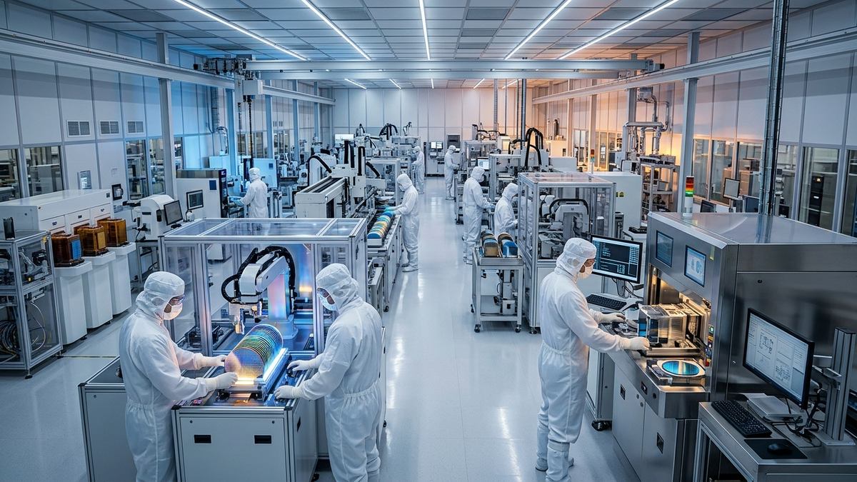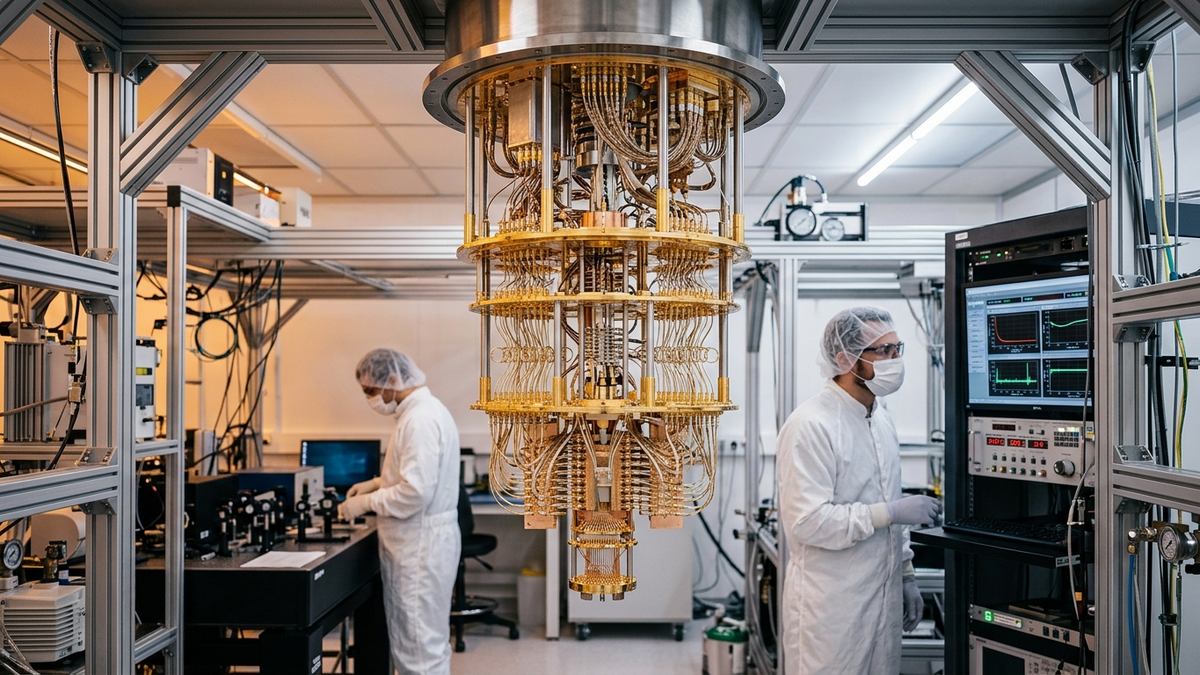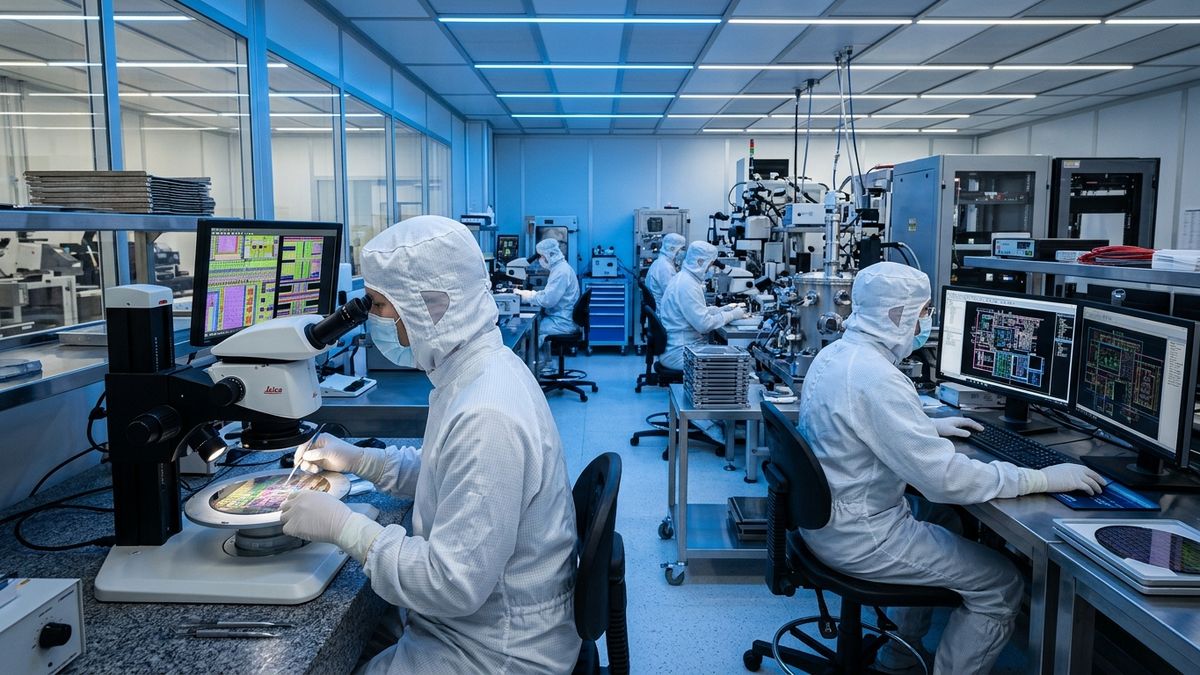
HCLTech and Japan's Rapidus launch advanced semiconductor design centres in Bengaluru and Hubli to power 2nm logic chip tape-outs and PDK development.
Executive Key Takeaways
- HCLTech and Japan's Rapidus Corporation inaugurated two dedicated semiconductor engineering development centres in Bengaluru and Hubli, Karnataka.
- The engineering hubs focus on sub-2-nanometer (2nm) logic manufacturing capabilities, spanning mask design, layout infrastructure, PDK development, and DTCO.
- The strategic initiative cements an India-Japan engineering corridor, supplying specialized VLSI design and microelectronics talent to Rapidus' Hokkaido mega-foundry.
Global technology services enterprise HCLTech has established a high-level strategic engineering alliance with Japan's advanced logic foundry venture Rapidus Corporation, inaugurating two dedicated semiconductor design and development centres in Bengaluru and Hubli, Karnataka. The dual engineering hubs will directly support Rapidus' ambitious roadmap to commercialize cutting-edge 2-nanometer (2nm) logic semiconductors at its state-of-the-art manufacturing facility in Chitose, Hokkaido.
The collaboration represents a critical milestone in India's semiconductor value chain evolution, transitioning domestic engineering capabilities from basic testing and physical verification into sub-2nm gate-all-around (GAA) microelectronics architectures. By integrating HCLTech's seasoned very-large-scale integration (VLSI) engineers with Rapidus' foundry ecosystem, the partnership cements a high-value technology bridge between India and Japan.
Navigating the Sub-2nm Frontier: GAA Architecture and DTCO
As silicon scaling approaches atomic limits, transitioning from conventional FinFET transistor geometries to nanosheet Gate-All-Around (GAA) structures introduces immense physical complexities. Managing quantum tunneling effects, parasitic capacitance, and extreme thermal density requires profound structural alignment between circuit designers and wafer fabrication physicists.
The HCLTech-Rapidus engineering centres will specialize in several high-complexity microelectronics disciplines:
- Design Technology Co-Optimization (DTCO): Simultaneously refining transistor cell libraries, standard layout rules, and fabrication chemistry to squeeze maximum clock speeds and power efficiency out of the 2nm silicon lattice.
- Process Design Kit (PDK) Development: Constructing, verifying, and distributing the foundational algorithmic rules and model files that global fabless chip designers use to map logic gates onto Rapidus' 2nm lithography process.
- Mask Synthesis & Layout Design: Developing ultra-precise optical proximity correction (OPC) masks and multi-layer metallization interconnects capable of extreme ultraviolet (EUV) lithography resolution.
- High-Bandwidth Memory (HBM) and Interposer Integration: Engineering 2.5D and 3D advanced packaging architectures that link 2nm logic dies directly to high-capacity memory stacks for next-generation AI accelerators.
"Commercializing 2nm semiconductor manufacturing requires an open, world-class collaborative ecosystem uniting premier design talent with state-of-the-art foundry execution,"stated executive leadership from Rapidus and HCLTech. "India's deep semiconductor talent pool, anchored by HCLTech's engineering rigor in Bengaluru and Hubli, plays an indispensable role in realizing our vision for rapid, energy-efficient silicon."
The expansion aligns with parallel industrial engineering breakthroughs across India's high-tech landscape, such as HCLTech's AI automotive simulation suites with NVIDIA and five-year industrial automation alliances with Nokia.
The Strategic Importance of Hubli as an Emerging Tier-2 Semiconductor Node
While Bengaluru has long served as India's undisputed capital for fabless chip design, HCLTech's deliberate decision to anchor a dedicated facility in Hubli marks an important decentralization milestone for Karnataka's deeptech ecosystem.
Hubli-Dharwad boasts premier academic institutions including the Indian Institute of Information Technology (IIIT Dharwad), IIT Dharwad, and BVB College of Engineering and Technology (KLE Technological University). By establishing advanced VLSI design cleanrooms in Hubli:
- HCLTech provides high-tier engineering graduates with cutting-edge microelectronics careers without necessitating relocation to saturated tier-1 metros.
- Operational infrastructure costs are reduced by 25% to 35% compared to Bengaluru, improving overall project delivery unit economics.
- The state government's "Beyond Bengaluru" policy gains tangible momentum, anchoring high-precision hardware research along the northern Karnataka industrial belt.
Technical Scope Matrix: Dual Semiconductor Centre Capabilities
The table below summarizes the operational allocations and technical specializations across the Bengaluru and Hubli engineering facilities:
| Technical Discipline | Primary Facility | Scope & Deliverables | Strategic Milestone |
|---|---|---|---|
| Process Design Kit (PDK) | Bengaluru Centre | Transistor modeling, SPICE simulation rules, GAA parameter libraries | Enable global fabless clients to tape-out on Rapidus 2nm lines |
| Design Technology Co-Optimization | Bengaluru Centre | Cell layout compaction, voltage scaling, parasitic capacitance minimization | Achieve targeted performance-per-watt thresholds for AI accelerators |
| Mask Infrastructure & Verification | Hubli Centre | Design rule checking (DRC), layout vs schematic (LVS), optical proximity modeling | Defect-free mask tape-out for EUV lithography scanners |
| Analog & Mixed-Signal Layout | Hubli Centre | Power delivery networks, clock tree synthesis, ultra-low-jitter PLL designs | High-reliability power distribution across multi-die packages |
| India-Japan Engineering Exchange | Both Hubs | Joint training rotations, foundry cross-skilling, bilingual technical roadmaps | Sustained pipeline of specialized sub-2nm Indian engineers |
Catalyzing Rapidus' Collaborative Open Rapid Ecosystem (CORE)
Unlike traditional foundry giants that rely on rigid, closed development models, Rapidus is spearheading the Collaborative Open Rapid Ecosystem (CORE) initiative. CORE brings together leading design houses, electronic design automation (EDA) software vendors, IP providers, and system integrators to drastically truncate turnaround times from architecture conception to physical wafer tape-out.
HCLTech's dual development centres in India serve as primary execution pillars within CORE. By providing end-to-end design infrastructure and rapid customer onboarding support, HCLTech enables global high-performance computing (HPC) clients, automotive Tier-1s, and sovereign defense contractors to transition designs onto Rapidus' 2nm production line smoothly.
Bolstering India's Semiconductor Mission (ISM)
From a macro perspective, the HCLTech-Rapidus agreement provides strong impetus to the India Semiconductor Mission (ISM). While the initial phase of the ISM has focused heavily on assembling packaging facilities (ATMP/OSAT) and legacy node wafer fabrication, participating in sub-2nm chip design elevates Indian engineers into the most sophisticated echelon of global silicon physics.
As these Indian engineers master the intricacies of GAA transistors, EUV lithography tolerances, and atomic-level interconnect dynamics, they cultivate the specialized human capital essential for India to eventually establish its own commercial leading-edge semiconductor foundries in the coming decade.
Frequently Asked Questions
What is the primary focus of the partnership between HCLTech and Rapidus?
The alliance focuses on developing specialized design infrastructure, layout engineering, Process Design Kits (PDK), and Design Technology Co-Optimization (DTCO) to support Rapidus' commercial 2nm chip manufacturing.
Where are the two new semiconductor engineering centres located in India?
The centres are located in Karnataka: one in the technology hub of Bengaluru, and the other in the tier-2 emerging engineering corridor of Hubli.
What is Rapidus Corporation and what is its global semiconductor objective?
Rapidus is Japan's state-backed semiconductor venture established by eight major industrial corporations to build an advanced 2nm logic semiconductor foundry in Chitose, Hokkaido.
What is Design Technology Co-Optimization (DTCO) in 2nm chip fabrication?
DTCO is a collaborative methodology where chip designers and semiconductor process engineers jointly optimize circuit layout rules and transistor physics simultaneously to maximize energy efficiency and silicon density.
Primary Sources & Official References
- HCL Technologies Limited: Corporate Disclosure & Stock Exchange Announcement
- Rapidus Corporation: Global Semiconductor Ecosystem & Partner Milestones
- India Semiconductor Mission (ISM): Bilateral Microelectronics Collaboration Framework
- Ministry of Economy, Trade and Industry of Japan (METI): Advanced Semiconductor Strategy