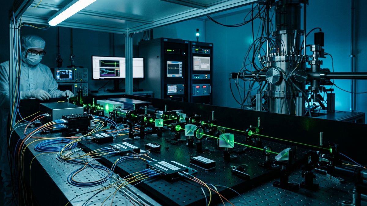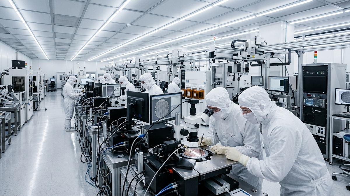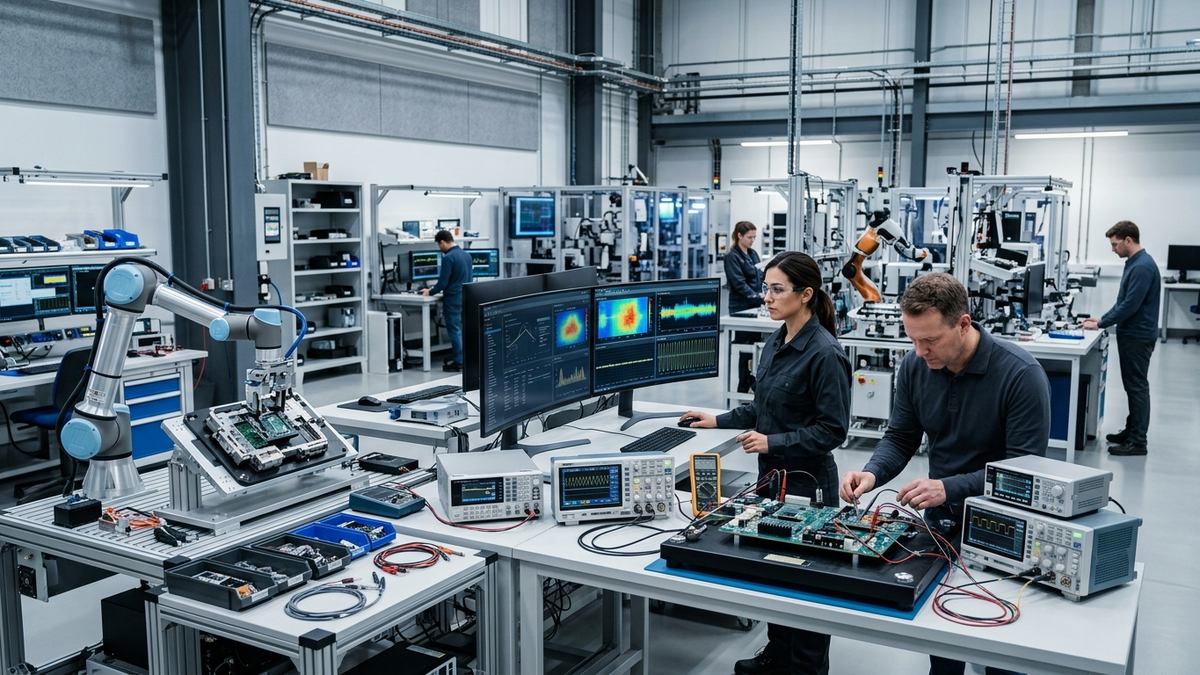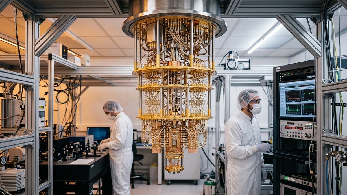
Samsung Semiconductor and the Indian Institute of Science partner to establish a state-of-the-art Quantum Research Lab in Bengaluru to pioneer solid-state quantum chips.
Executive Key Takeaways
- Samsung Semiconductor and the Indian Institute of Science (IISc) have established a joint Quantum Research Lab in Bengaluru to develop solid-state quantum computing hardware.
- The state-of-the-art facility features dilution refrigerator cryostats capable of cooling quantum circuits down to near-absolute zero (10 millikelvin).
- Research initiatives focus on silicon spin qubits, cryogenic CMOS interface chips, and post-quantum cryptographic security directly aligned with India's National Quantum Mission.
Samsung Semiconductor, the microelectronics and silicon manufacturing division of Samsung Electronics, has formally partnered with the Indian Institute of Science (IISc) to establish a joint Quantum Technology Research Laboratory at the IISc campus in Bengaluru. The landmark collaboration brings together one of the world's largest commercial semiconductor foundries and India's preeminent research university to tackle one of the most demanding engineering frontiers of the twenty-first century: scalable solid-state quantum computing.
The new facility is equipped with state-of-the-art cryogenic dilution refrigerators operating at near-absolute zero (10 millikelvin), atomic-scale characterization tools, and precision microwave control apparatus. By marrying Samsung's world-leading sub-2nm silicon fabrication, extreme ultraviolet (EUV) lithography, and advanced 3D packaging capabilities with IISc's celebrated faculty in quantum physics, condensed matter theory, and materials engineering, the partnership aims to develop practical, fault-tolerant quantum processors built upon standard silicon CMOS architectures.
Silicon Spin Qubits: Leveraging Standard Semiconductor Foundries for Quantum Scale
While early commercial quantum systems developed by multinational tech giants have largely relied on superconducting circuits or trapped ion chambers, these architectures encounter massive scaling bottlenecks when transitioning from hundreds to millions of physical qubits. Superconducting systems require vast physical footprints and massive coaxial wiring harnesses that become unwieldy at scale.
In contrast, the Samsung-IISc research charter concentrates primarily on silicon spin qubits—often referred to as "quantum dots." Because spin qubits trap individual electron spins within nanometer-scale silicon quantum wells, their physical dimensions are thousands of times smaller than superconducting resonators.
Crucially, silicon spin qubits can be fabricated using the same cleanroom equipment, chemical vapor deposition systems, and photolithography tools already deployed in commercial semiconductor foundries. This opens the historic possibility of manufacturing quantum chips alongside classical processors on 300mm silicon wafers.
"Quantum computing has transitioned from the realm of speculative physics into a grueling semiconductor engineering challenge,"said senior research directors at IISc's Centre for Nano Science and Engineering (CeNSE). "Designing millions of uniform quantum dots requires the world's most disciplined nanometer-scale lithography and materials purity. Samsung's foundry mastery paired with IISc's fundamental quantum optics research creates an ideal ecosystem to establish sovereign quantum capability in India."
This academic-industry alliance reinforces the expanding domestic deeptech foundation, complementing the semiconductor packaging and testing expansions documented in /post/tessolve-raises-75-million-for-semiconductor-expansion.
Cryogenic CMOS: Overcoming the Thermal Interconnect Bottleneck
A critical technical bottleneck in modern quantum computing is the "wiring problem." While the quantum processor core must be maintained at 10 millikelvin (-273.14°C) inside a dilution refrigerator to prevent thermal decoherence, the classical electronic instruments that read and control the qubits typically sit at room temperature (300 Kelvin), connected via hundreds of individual coaxial cables that introduce thermal leakage and signal noise.
The Samsung-IISc lab is addressing this limitation by co-designing Cryogenic CMOS (cryo-CMOS) integrated circuits. These specialized mixed-signal silicon chips are engineered to operate reliably at 4 Kelvin inside the cryostat, generating control pulses and digitizing readout signals right next to the quantum chip, slashing wiring density by over 90%.
Strategic Research Tracks: IISc-Samsung Quantum Laboratory
The structured table below details the four primary research thrusts, technical milestones, and industrial applications established under the joint charter:
| Research Track | Core Technical Focus | Primary Engineering Challenge | Target Milestone / Deliverable |
|---|---|---|---|
| Silicon Quantum Dots | Electron and hole spin qubits in isotopically pure Silicon-28 | Charge noise reduction and uniform valley splitting | Multi-qubit silicon array with >99.5% two-qubit gate fidelity |
| Cryogenic CMOS Control | Mixed-signal controller ICs operating at 4 Kelvin | Sub-milliwatt power dissipation inside cryostat | Turnkey cryogenic qubit control ASIC with integrated DACs/ADCs |
| Advanced 3D Packaging | Heterogeneous 3D chiplet stacking for quantum systems | Superconducting through-silicon vias (TSVs) | Cryogenic multichip module with zero thermal interconnect leakage |
| Post-Quantum Cryptography | Hardware accelerators for quantum-resistant algorithms | Lattice-based cryptographic math optimization | Silicon IP core compliant with NIST post-quantum standards |
Synergies with India's National Quantum Mission (NQM)
The establishment of the Samsung-IISc laboratory directly accelerates the mandates of the National Quantum Mission (NQM), approved by the Union Cabinet under the Department of Science and Technology (DST). With a budgetary allocation exceeding ₹6,000 crore, the NQM aims to build intermediate-scale quantum computers with 50 to 1,000 physical qubits within the decade.
By establishing an open collaborative platform in Bengaluru, the lab will train scores of doctoral candidates, postdoctoral researchers, and semiconductor design engineers in quantum device physics, creating a talent pipeline capable of servicing both domestic institutions and global technology corporations.
This high-tech deployment complements other landmark scientific and supercomputing initiatives across the subcontinent, such as the regional quantum infrastructure projects explored in /post/ibm-to-bring-quantum-computing-to-amaravati.
Furthermore, as enterprise software vendors and hyperscale cloud operators race to adopt post-quantum cryptographic defenses—such as the digital infrastructure investments highlighted in /post/jio-sets-price-band-for-indias-biggest-ever-ipo—the Samsung-IISc Quantum Research Lab positions Bengaluru as a preeminent hub for next-generation quantum silicon engineering.
Frequently Asked Questions
What is the primary objective of the Samsung Semiconductor and IISc Quantum Research Lab?
The joint laboratory aims to accelerate the commercialization of solid-state quantum computing by combining Samsung's advanced semiconductor fabrication and 3D packaging expertise with IISc's pioneering research in quantum physics, materials science, and cryogenic device characterization.
Where is the new quantum facility located and what equipment does it house?
The lab is established inside the Indian Institute of Science campus in Bengaluru. It houses ultra-low-noise dilution refrigerator cryostats capable of operating at 10 millikelvin, high-frequency microwave signal generators, and specialized cleanroom test fixtures for measuring quantum spin states.
Why is the collaboration focusing on silicon spin qubits instead of superconducting loops?
Silicon spin qubits leverage existing industrial semiconductor fabrication infrastructure (CMOS), meaning quantum processors could theoretically be manufactured in standard commercial fabs rather than requiring entirely novel bespoke manufacturing pipelines.
How does this joint lab support India's National Quantum Mission (NQM)?
The partnership directly advances the National Quantum Mission's goal of establishing domestic quantum technology leadership by training specialized quantum engineers, securing sovereign intellectual property, and establishing local cleanroom characterization capabilities.
Primary Sources & Official References
- Indian Institute of Science (IISc): Directorate of Research and Industry Collaborations - Samsung Quantum Lab Charter.
- Samsung Semiconductor Global Research: Advanced Silicon Qubit Architecture and Cryogenic Electronics Briefings.
- Department of Science and Technology (DST): National Quantum Mission Guidelines and Quantum Computing Hub Milestones.
- India Semiconductor Mission (ISM) / MeitY: Advanced R&D and Academic-Industry Semiconductor Frameworks.