India Accelerates Semiconductor Push: Industry Leaders and IIT Delhi Join Forces to Scale Fabless Chip-Design Startups
By Rohan Varma | Published August 3, 2026 | 9 min read
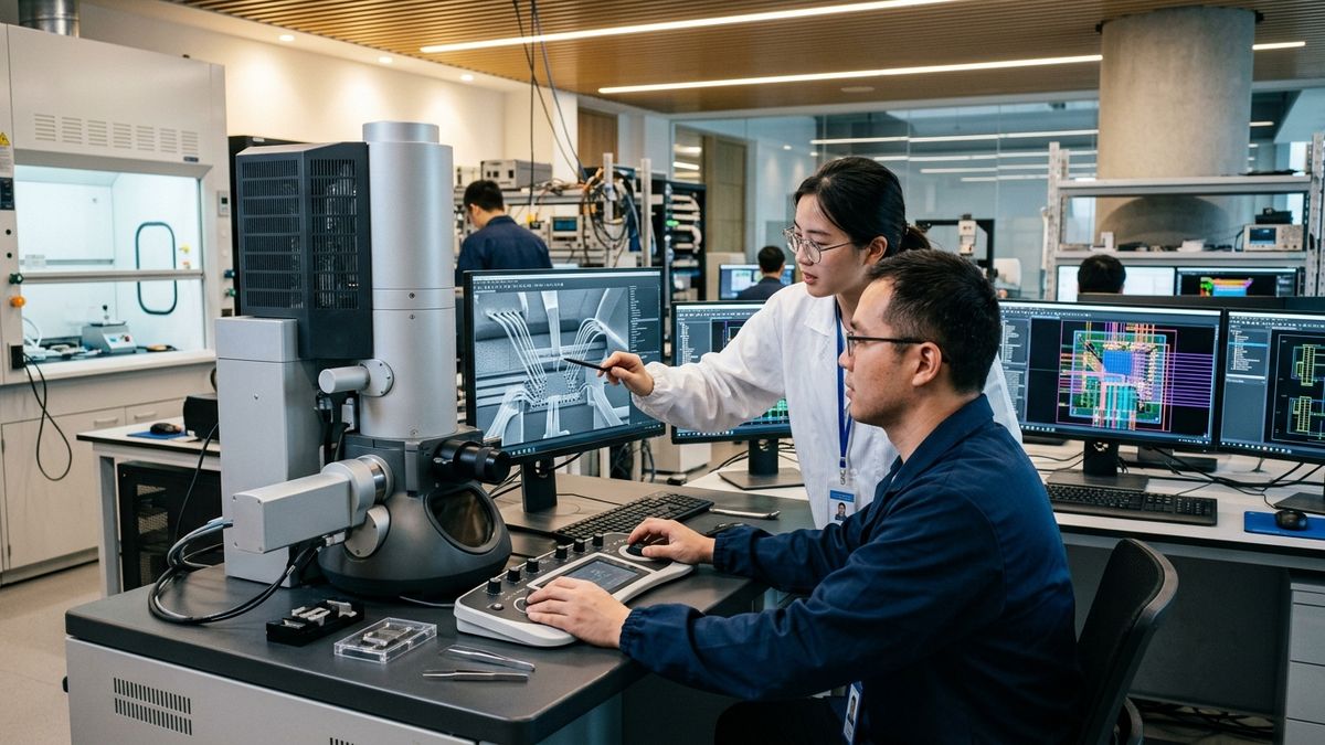
IIT Delhi collaborates with industry pioneers to power India's fabless semiconductor ecosystem, nurturing domestic chip design ventures and technological sovereignty.
In a strategic effort to cement India's position as a global microelectronics powerhouse, leading semiconductor industry titans have joined forces with IIT Delhi to launch an ecosystem accelerator for fabless chip-design startups. This high-impact collaboration aims to nurture homegrown chip entrepreneurs, develop sovereign semiconductor intellectual property (IP), reduce national reliance on imported silicon, and fortify India's role in global deep-tech supply chains.
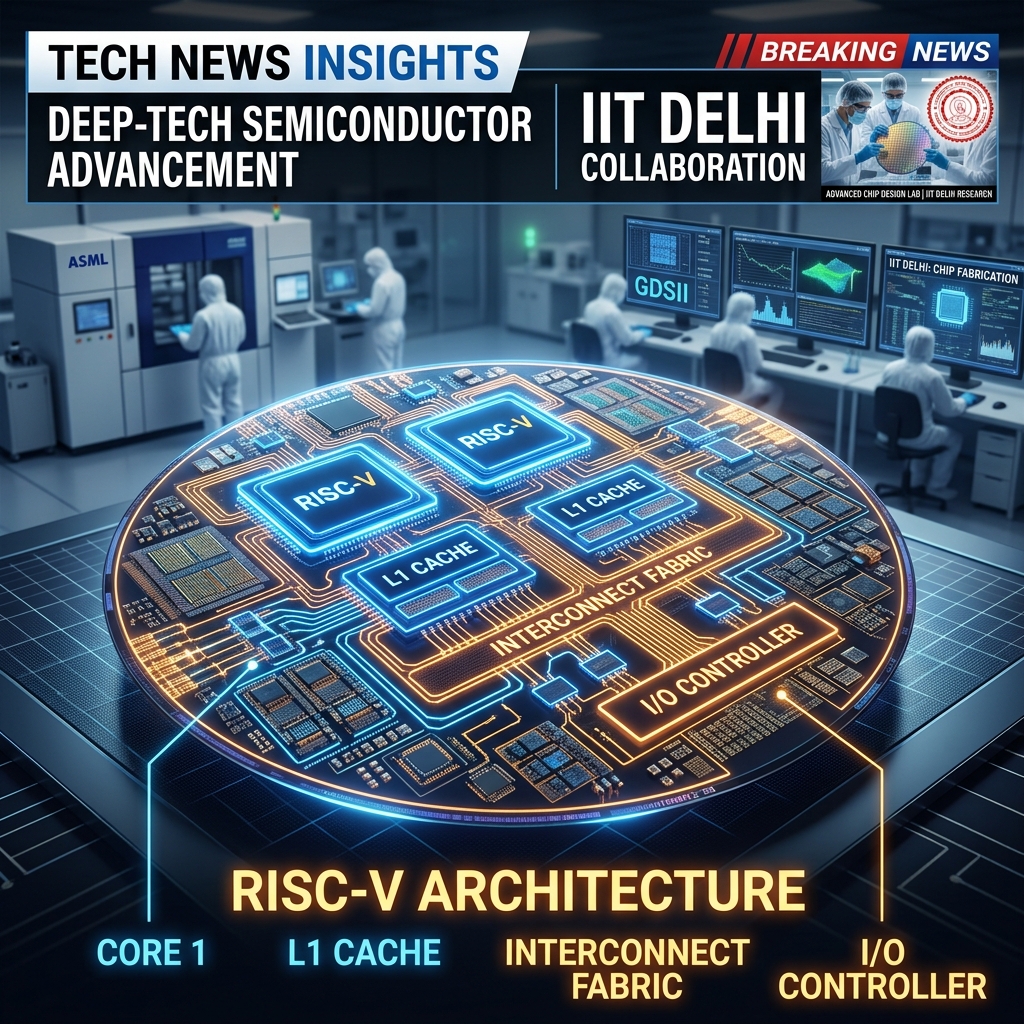
By focusing aggressively on the fabless model—where domestic ventures design advanced microchips, System-on-Chips (SoCs), and RISC-V architectures while partnering with global semiconductor foundries for fabrication—India is leveraging its world-class engineering talent to build high-margin technological IP without incurring the multi-billion-dollar upfront capital costs of physical fab construction.
The Fabless Model: India's High-Leverage Semiconductor Strategy
India has long been recognized as a global hub for semiconductor design talent, with over 20% of the world's chip design workforce operating out of domestic R&D centers for global tech giants. However, historical gaps in seed funding, expensive Electronic Design Automation (EDA) software licenses, and limited prototyping access prevented Indian engineers from launching their own chip startups.
The IIT Delhi semiconductor partnership directly resolves these systemic bottlenecks by establishing a shared infrastructure hub that grants early-stage ventures access to enterprise EDA design suites, Multi-Project Wafer (MPW) prototyping runs, advanced testing labs, and industry mentorship.
Core Objectives of the IIT Delhi & Industry Semiconductor Alliance
1. Democratic Access to EDA Tooling: Providing early-stage founders with subsidized licenses for industry-standard Cadence, Synopsys, and Siemens EDA design suites.
2. MPW Prototyping Subsidies: Pooling chip designs onto shared wafer runs, reducing physical prototype fabrication costs by up to 80% for early-stage startups.
3. RISC-V Ecosystem Expansion: Accelerating open-source RISC-V processor architecture development tailored for IoT, automotive, industrial automation, and defense applications.
This iniciativa complements major hardware milestones across India, including Gujarat's SemTech RISC-V IoT chip design breakthough, Skyroot's aerospace semiconductor integration, and government capital infusions via the Electronics Development Fund.
Fabless Chip Architecture & Ecosystem Growth Matrix
The alliance between academia and industry sets concrete operational and technological benchmarks to scale India's fabless ecosystem. The matrix below outlines key focus areas and strategic execution vectors.
| Semiconductor Focus Area | Target Milestone / Capability | Strategic Ecosystem Execution Vector |
|---|---|---|
| EDA Tooling Access | Cloud-hosted design clusters at IIT Delhi | Eliminates $500K+ initial software license cost for startups |
| Architecture Standard | Custom RISC-V & ARM SoCs | Tailored for edge AI, smart meters, automotive, & 5G/6G |
| Prototyping Turnaround | MPW Shuttles via Global Fabs | Accelerates silicon tape-out from 18 months down to 6 months |
| Foundry Partnership | Alliances with TSMC, GlobalFoundries, & Local Fabs | Seamless transition from prototype tape-out to volume production |
| Talent & R&D Pipeline | 500+ M.Tech & PhD Chip Engineers | Direct pipeline from university labs to fabless startup founders |
Academic Rigor Meets Industry Execution
The collaboration brings together senior chip architects, silicon venture capitalists, and IIT Delhi's world-class microelectronics faculty. Participating startups receive hands-on guidance on physical design, timing closure, thermal management, and post-silicon validation.
"India possesses world-class chip design talent. By creating a collaborative ecosystem with IIT Delhi that offers access to expensive EDA software, silicon prototyping, and venture capital, we are enabling Indian engineers to build the global semiconductor giants of tomorrow,"stated a leading semiconductor industry executive involved in the initiative.
Strategic Alignment with India's Semiconductor Sovereignty
This fabless initiative aligns perfectly with national priorities under the India Semiconductor Mission (ISM) and the Design Linked Incentive (DLI) scheme. By nurturing domestic chip companies capable of producing microcontrollers, power management ICs, and AI accelerator chips, India is building long-term technological self-reliance.
As fabless startups nurtured at IIT Delhi move from tape-out to mass production, India is poised to transform from a consumer of global silicon into an indispensable supplier of advanced chip designs for the global tech economy.
#Semiconductors #ChipDesign #DeepTech #IITDelhi #StartupEcosystem #MadeInIndia #TechForIndia #InnovationLeadership #IndiaRising #FutureOfTech