Bengaluru-based Tessolve secures $75 million in growth funding to acquire specialized chip-design houses and scale automated semiconductor test engineering facilities.
Executive Key Takeaways
- Tessolve has secured $75 million in fresh growth capital to expand its turnkey semiconductor design, post-silicon validation, and testing infrastructure.
- The proceeds will finance targeted acquisitions of analog and mixed-signal design firms in North America and Europe, while expanding cleanroom test capacity in Bengaluru and Hyderabad.
- The investment reinforces India's pivotal role in global semiconductor value chains under the India Semiconductor Mission (ISM).
Bengaluru-headquartered semiconductor engineering solutions leader Tessolve Semiconductor has secured $75 million in fresh growth funding to fuel strategic global acquisitions, expand automated test equipment (ATE) facilities, and scale turnkey silicon engineering services. The substantial capital raise arrives at a critical inflection point as the worldwide semiconductor industry races to navigate the unprecedented complexities of sub-3nm chip fabrication, 2.5D/3D advanced chiplet packaging, and high-volume post-silicon validation.
Backed by prominent private equity partners and parent technology conglomerate Hero Electronix, Tessolve plans to deploy the proceeds to acquire boutique analog and mixed-signal chip design consultancies across North America and Europe, while aggressively expanding cleanroom test engineering capacity across its primary engineering centers in Bengaluru, Hyderabad, and Coimbatore.
The Critical Post-Silicon Bottleneck: Why Test Engineering Dictates Time-to-Market
While public attention often centers on semiconductor fabrication mega-foundries (fabs) like TSMC, Intel, or Samsung, the journey from raw silicon wafer to a functioning commercial processor is heavily dependent on post-silicon engineering. As chip designs incorporate billions of transistors across heterogenous chiplet architectures, the risk of latent manufacturing flaws, thermal cross-talk, and signal integrity degradation escalates exponentially.
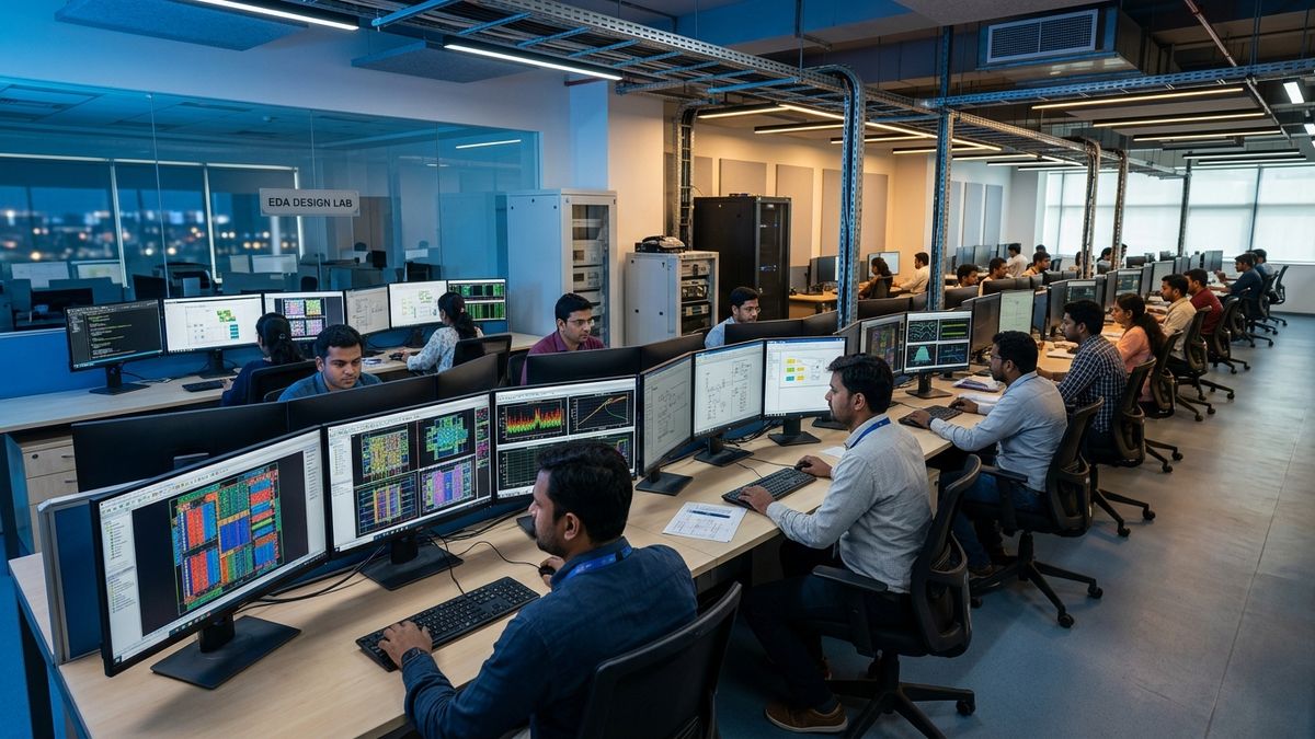
A single undetected silicon flaw can delay an automotive or AI processor launch by 9 to 12 months, resulting in hundreds of millions of dollars in lost market revenue. Tessolve bridges this mission-critical gap by providing comprehensive end-to-end semiconductor services—spanning initial RTL specification, physical design, design-for-test (DFT), test program generation, loadboard hardware design, and round-the-clock silicon characterization.
"Global fabless semiconductor enterprises are facing historic engineering bottlenecks,"said senior semiconductor testing executives. "Designing a microchip is only half the commercial battle; proving that it operates reliably across extreme voltage and temperature fluctuations before mass fabrication is where enterprise success is determined. Tessolve's expanded capital base allows us to offer turnkey post-silicon validation at global scale."
This expansion reflects the deepening domestic hardware and advanced engineering ecosystem in India, paralleling the precision manufacturing breakthroughs documented in /post/thinkmetal-raises-27-crore-for-manufacturing-innovation.
Strategic Acquisition Roadmap and Lab Infrastructure Expansion
Tessolve's $75 million capital deployment strategy focuses on two distinct growth vectors designed to cement its leadership among independent semiconductor engineering service providers:
1. Targeted Cross-Border Acquisitions in Analog and Automotive Silicon
A substantial allocation of the growth capital will finance targeted acquisitions of boutique semiconductor design houses in North America and Europe. These acquisitions will specifically target specialized engineering talent in high-voltage power management integrated circuits (PMICs), automotive functional safety (ISO 26262), and RF/wireless transceiver design, expanding Tessolve's high-margin client relationships with top-tier automotive tier-1 suppliers and industrial automation leaders.
2. Doubling Cleanroom Automated Test Equipment (ATE) Capacity
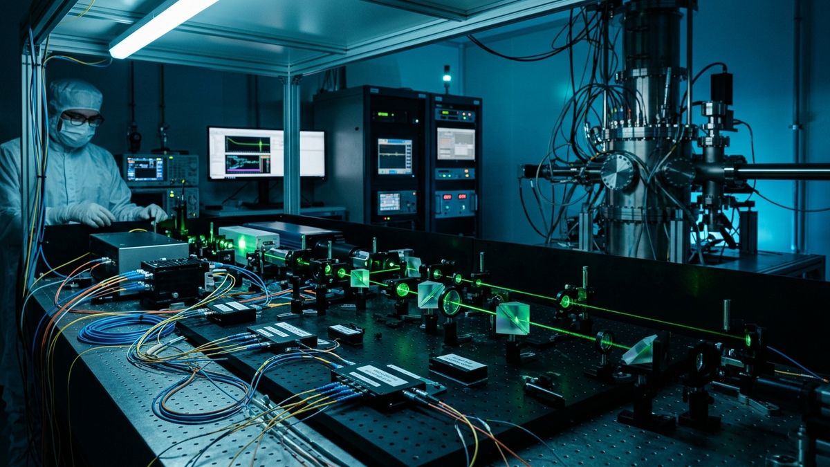
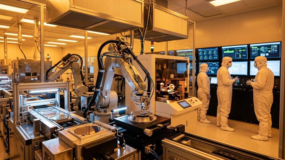
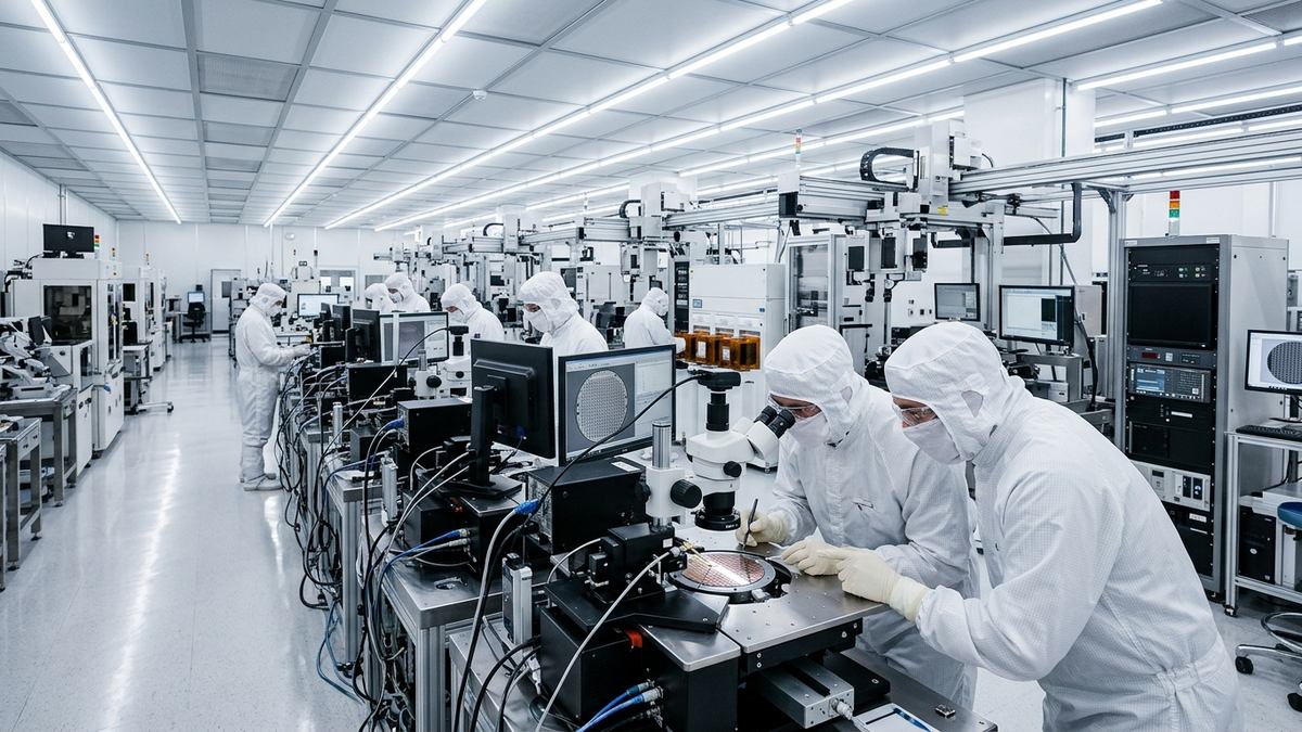
Testing modern high-speed AI processors and automotive microcontrollers requires multi-million-dollar automated test platforms from manufacturers like Advantest and Teradyne. Tessolve is expanding its certified cleanroom laboratories, installing next-generation high-pin-count digital testers, RF test bays, and automated wafer probers to provide 24/7 silicon characterization services to multinational fabless clients.
Semiconductor Engineering Service Matrix: Capabilities and Growth Vectors
The structured table below outlines Tessolve's end-to-end service capabilities across the semiconductor product lifecycle:
| Engineering Phase | Core Technical Capabilities | Primary Industry Drivers | Tessolve Strategic Focus Area |
|---|---|---|---|
| Pre-Silicon Design & Verification | RTL coding, UVM verification, physical design, synthesis, timing closure | AI accelerator complexity, migration to 3nm and 2nm nodes | Turnkey ASIC development and IP subsystem integration |
| Design for Testability (DFT) | Scan insertion, BIST (Built-In Self-Test), ATPG, boundary scan | High defect coverage requirements in automotive and aerospace | Automated fault grading and zero-defect automotive qualification |
| Hardware Engineering | ATE loadboard design, probe card PCB layout, high-frequency signal integrity | Complex multi-layer PCBs (>50 layers) operating above 50 GHz | High-density loadboards for 2.5D/3D chiplet packages |
| Post-Silicon Validation & ATE Test | Silicon bring-up, wafer sort testing, final package test programming, thermal characterization | Hyperscale data center compute, extreme reliability testing | 24/7 test floor execution across Advantest & Teradyne platforms |
| Embedded System Solutions | System-on-Module (SoM) design, firmware development, edge AI integration | Industrial IoT, autonomous robotics, smart medical hardware | Turnkey commercial module manufacturing and carrier boards |
Synergies with the India Semiconductor Mission (ISM)
Tessolve's expansion directly aligns with the strategic objectives of the India Semiconductor Mission (ISM), supported by MeitY. With multiple commercial semiconductor fabrication and assembly-test-marking-pack (ATMP/OSAT) facilities currently under construction across Gujarat and Assam—such as the Tata Electronics and CG Power ventures—domestic availability of world-class test and characterization engineering is essential for building a self-sustaining semiconductor ecosystem.
This growing domestic infrastructure capability complements other landmark technology deployments across the subcontinent, such as the advanced hardware hubs covered in /post/ibm-to-bring-quantum-computing-to-amaravati.
Furthermore, as global tech giants establish sovereign data centers and electronic manufacturing alliances—highlighted in /post/adani-and-jabil-join-forces-for-ai-infrastructure—independent engineering powerhouses like Tessolve provide the specialized technical foundation necessary to design, validate, and certify mission-critical silicon on domestic soil.
Frequently Asked Questions
What is Tessolve and what semiconductor services does it provide?
Tessolve Semiconductor is a global semiconductor engineering solution provider that offers full turnkey services, including ASIC chip design, design-for-test (DFT), automated test equipment (ATE) software development, PCB loadboard hardware design, and post-silicon validation.
How much capital has Tessolve raised and who backed the round?
Tessolve secured $75 million in growth financing, backed by prominent institutional private equity investors alongside continuing strategic support from its parent company, Hero Electronix.
Why is post-silicon validation and testing so critical in modern chip design?
Modern processors built on sub-3nm nodes contain billions of interconnected transistors. Post-silicon validation verifies that the physical silicon functions flawlessly under diverse thermal, voltage, and electrical stress conditions before high-volume commercial production begins.
How does Tessolve's expansion support the India Semiconductor Mission (ISM)?
As India builds out its domestic chip fabrication and OSAT packaging infrastructure, Tessolve provides the essential high-level design, testing, and validation engineering talent required to service both domestic fabs and international fabless chip design clients.
Primary Sources & Official References
- Tessolve Semiconductor Corporate Disclosures: Strategic Growth Financing and International Acquisition Roadmaps.
- Hero Electronix Corporate Statements: Electronics & Deeptech Venture Capital Allocations.
- India Semiconductor Mission (ISM) / Ministry of Electronics and Information Technology (MeitY): Semiconductor Policy Guidelines and Ecosystem Development Metrics.
- SEMI (Semiconductor Equipment and Materials International): Global Semiconductor Test Equipment and Silicon Packaging Outlook.