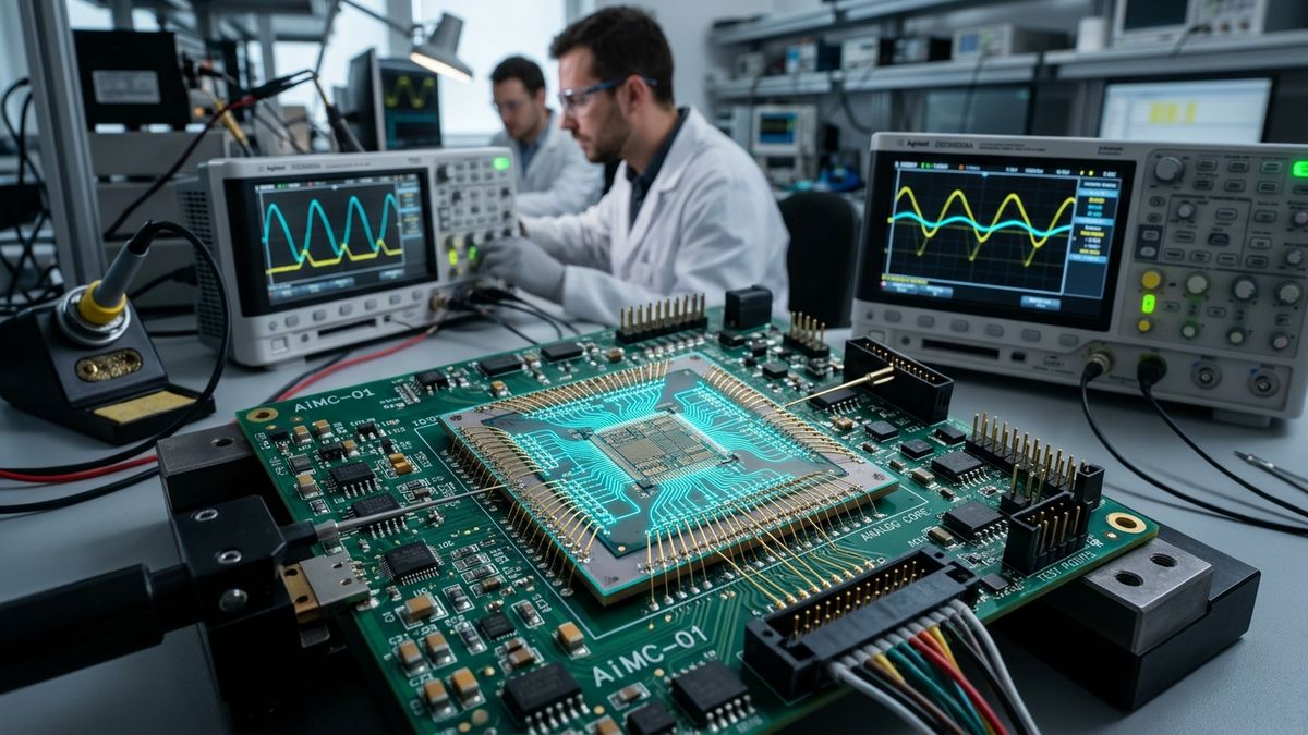
Indian AI Chip Startup Netrasemi Unveils Indigenously Designed 12nm Edge-AI SoC for Robotics, Drones, and Smart Mobility
By Rohan Varma | Published September 29, 2026 | 8 min read
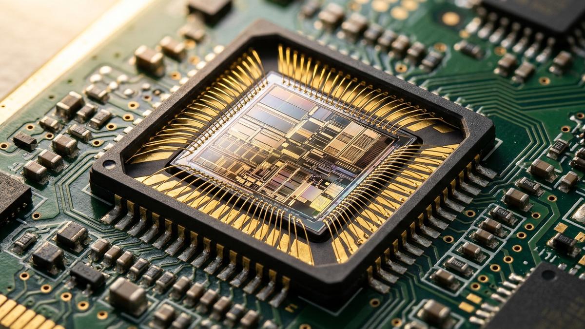
Fabless semiconductor startup Netrasemi demonstrates an indigenously engineered 12nm Edge-AI SoC, delivering high-efficiency neural compute for drones, surveillance, and robotics.
Indian fabless semiconductor startup Netrasemi has formally unveiled its indigenously engineered 12nm Edge-AI System-on-Chip (SoC), marking a monumental milestone for India's domestic microelectronics design capabilities. Demonstrating live silicon in high-throughput computer vision benchmarks, Netrasemi proved that Indian hardware architects can design commercially competitive, high-efficiency neural accelerators capable of running complex deep learning models directly on edge devices—ranging from smart surveillance cameras and autonomous delivery drones to industrial collaborative robots and intelligent automotive mobility platforms.
The demonstration arrives at a pivotal juncture for the global semiconductor landscape. As cloud computing costs escalate and privacy regulations tighten, enterprises are aggressively moving machine learning inference from centralized data centers to the physical "edge"—the devices collecting data in the real world.
By successfully designing and taping out a 12nm FinFET System-on-Chip, Netrasemi directly challenges global semiconductor stalwarts like Ambarella, Hailo, and Nvidia's edge divisions, proving that India's deeptech ecosystem can produce world-class silicon intellectual property (IP).
The Edge Computing Imperative: Why Cloud AI Fails Real-Time Hardware
While large language models (LLMs) running in hyperscale data centers dominate public headlines, physical machines operating in the physical world cannot depend on remote cloud connections.
Autonomous drones flying at 60 km/h, industrial robotic arms assembling circuit boards, and smart surveillance cameras scanning security perimeters operate under strict constraints:
1. Network Latency and Disconnection: A drone navigating through tree canopies or an automated guided vehicle (AGV) in a steel warehouse cannot afford a 200-millisecond latency roundtrip to a cloud server to determine if an obstacle is present. Network drops cause physical collisions.
2. Bandwidth Costs: Streaming continuous 4K 60fps video feeds from thousands of smart city cameras to cloud data centers consumes astronomical bandwidth and incurs prohibitive cloud storage fees.
3. Power and Thermal Budgets: Edge devices operate on small lithium-ion batteries or passive cooling enclosures. They cannot support power-hungry 150-watt desktop GPUs; they require neural inference engines operating between 1 watt and 5 watts.
Netrasemi's 12nm Edge-AI SoC addresses these precise operational realities by delivering high-throughput neural inference within a compact thermal envelope.
"True physical artificial intelligence must happen locally, deterministically, and with minimal power consumption,"explained Netrasemi's architectural leadership. "Our 12nm SoC is designed from the silicon gates up to deliver maximum neural operations per watt, empowering domestic drone makers, robotics labs, and camera manufacturers to deploy intelligent autonomy without sending a single byte of video to external cloud servers."
Architectural Breakdown: Netrasemi 12nm Edge-AI SoC
Netrasemi's silicon combines custom neural hardware accelerators, high-throughput image signal processors (ISP), and open-standard control cores into a unified heterogeneous architecture:
| Silicon Subsystem | Microarchitecture Specification | Functional Capability |
|---|---|---|
| Manufacturing Process | 12nm FinFET Process Node | Optimized balance between transistor density, wafer cost, and power efficiency |
| Neural Processing Unit (NPU) | Custom Multi-Core Tensor Architecture | Delivering 4 to 12 INT8/FP16 TOPS at sub-3W operational power consumption |
| Image Signal Processor (ISP) | High-Dynamic Range (HDR) Vision Engine | Simultaneous processing of multiple 4K 60fps video streams with low-light enhancement |
| Control CPU Cores | Multi-Core 64-bit RISC-V Cluster | Real-time sensor arbitration, peripheral control, and application execution |
| Memory Subsystem | LPDDR4x / LPDDR5 High-Speed Bus | High-bandwidth memory interconnect preventing memory-bound neural stalls |
| Security Subsystem | Hardware Root of Trust & Cryptographic Engine | Secure boot, encrypted firmware storage, and anti-tamper silicon protections |
Target Applications: Robotics, Drones, and Smart Mobility
The commercial applications for Netrasemi's 12nm SoC span high-growth industrial verticals where edge intelligence is rapidly becoming mandatory:
- Autonomous Drones and Cargo Logistics: Providing real-time visual inertial odometry (VIO), dynamic obstacle avoidance, and precision landing without reliance on GPS signals in contested environments.
- Smart Security and City Surveillance: Executing real-time facial recognition, license plate reading, crowd anomaly detection, and perimeter violation alerts directly on the camera pole.
- Industrial Robotics and Factory Automation: Powering multi-axis robotic arms with high-precision computer vision for pick-and-place sorting, weld quality inspection, and worker proximity safety monitoring.
- Automotive Driver Assistance (ADAS): Supporting forward collision warning, pedestrian detection, lane departure telemetry, and driver drowsiness monitoring for commercial fleets and electric two-wheelers.
To understand how orbital satellites are similarly deploying edge AI computing into low Earth orbit to process imagery in real time, see our feature on /post/takeme2space-targets-orbital-ai-computing-moi-1a-spacex.
Silicon Sovereignty and the Design Linked Incentive (DLI)
Netrasemi's breakthrough is a crowning achievement for India's Design Linked Incentive (DLI) scheme, a core pillar of the India Semiconductor Mission (ISM) administered by MeitY. The DLI scheme was formulated specifically to nurture domestic fabless chip startups by subsidizing electronic design automation (EDA) software licenses, silicon shuttle runs, and expensive mask fabrication costs.
Historically, India's defense sector, commercial drone manufacturers, and surveillance providers relied almost exclusively on imported chips from Western or Chinese vendors. This created grave vulnerabilities, including the risk of supply chain export embargoes and malicious silicon-level hardware backdoors.
By designing the silicon architecture indigenously and leveraging open-standard RISC-V instruction sets, Netrasemi provides a sovereign, secure computing foundation for Indian aerospace, defense, and civilian infrastructure.
To review how the broader semiconductor ecosystem is advancing across packaging, foundries, and materials, read /post/indias-semiconductor-push-expands-beyond-chip-design-semicon-india.
Future Roadmap
Following successful silicon demonstration and initial client evaluation kits, Netrasemi is gearing up for mass production qualification. The company is actively collaborating with domestic electronics manufacturing services (EMS) partners and system integrators to package the SoC into compact System-on-Modules (SoMs) for rapid adoption by original equipment manufacturers (OEMs).
As edge AI chips become the ubiquitous brains of the autonomous physical world, Netrasemi's silicon triumph proves that India's microelectronics future will be defined not just by assembly plants, but by high-value, homegrown intellectual property.
Frequently Asked Questions
What is Netrasemi and what did the company demonstrate?
Netrasemi is an Indian fabless semiconductor startup that designs high-efficiency edge AI processors. The company unveiled an indigenously architected 12nm Edge-AI System-on-Chip (SoC) capable of executing real-time deep learning computer vision and multimodal sensor fusion on battery-powered edge devices.
What are the core technical specifications of Netrasemi's 12nm SoC?
The chip is fabricated on a proven 12nm FinFET process node, integrating dedicated Neural Processing Units (NPUs), hardware video accelerators capable of multi-channel 4K stream processing, and real-time RISC-V control cores operating within a strict low-power budget of under 5 watts.
How does Netrasemi compare to global edge AI chips like Nvidia Jetson or Ambarella?
While global platforms like Nvidia Jetson offer broad general-purpose GPU compute at higher power consumption (10W–30W) and premium cost, Netrasemi's SoC is custom-architected for vision-first edge inference, delivering higher TOPS per watt and lower bill-of-materials (BOM) cost for high-volume commercial cameras, drones, and robots.
How does this breakthrough support India's semiconductor and defense sovereignty?
Historically, Indian surveillance cameras, commercial drones, and industrial robots relied entirely on imported silicon from the US, Taiwan, or China. Netrasemi's indigenous silicon design eliminates supply chain embargo risks, prevents hardware backdoors, and qualifies for the government's Design Linked Incentive (DLI) scheme.
Primary Sources & Official References
- Netrasemi Silicon Architecture Whitepaper: 12nm Edge-AI SoC Microarchitecture and Benchmark Metrics
- Ministry of Electronics and Information Technology (MeitY): Design Linked Incentive (DLI) Scheme Review
- IEEE Solid-State Circuits Society: Energy-Efficient Neural Processing Units for Autonomous Edge Devices
- Maker Village & Technopark Kerala: Hardware Incubator DeepTech Demonstration Registry