India's Semiconductor Push Expands Beyond Chip Design: SEMICON India 2026 Highlights Packaging, Foundries, and Materials Supply Chain
By Karthik Ramaswamy | Published September 29, 2026 | 8 min read
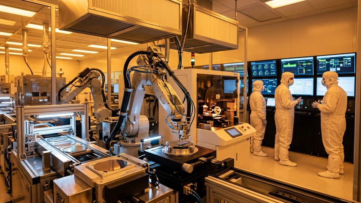
SEMICON India 2026 demonstrates India's decisive expansion from fabless chip design into commercial wafer fabrication, 2.5D/3D advanced packaging, and specialty materials.
SEMICON India 2026, the premier international semiconductor conference and exposition, concluded with a decisive demonstration of India's structural transformation from a design-centric talent pool into a comprehensive, full-stack microelectronics manufacturing nation. For over three decades, India's contribution to the global $600 billion semiconductor industry was confined almost exclusively to fabless chip design and verification. Today, multi-billion-dollar groundbreakings, cleanroom commissioning, and auxiliary chemical infrastructure are proving that the nation is building physical silicon capabilities across the entire value chain.
Organized under the auspices of the Ministry of Electronics and Information Technology (MeitY) and the India Semiconductor Mission (ISM), SEMICON India 2026 brought together over 300 global semiconductor executives, equipment fabricators, materials suppliers, and sovereign policy leaders.
The overarching consensus was unmistakable: while the world recognized India's engineering intellect, the operationalization of commercial wafer fabs, advanced packaging plants, and critical auxiliary infrastructure is cementing India's status as a critical node in global supply chain diversification.
The Design Baseline: India's Undisputed Silicon Intellect
India's physical semiconductor ambitions do not begin from scratch; they stand upon an extraordinarily robust engineering foundation. Over the past twenty-five years, every major semiconductor multinational—including Intel, Qualcomm, Nvidia, AMD, MediaTek, Texas Instruments, and Broadcom—established massive research and development centers across Bengaluru, Hyderabad, Noida, and Pune.
Today, India commands:
- Over 20% of the Global Chip Design Workforce: More than 125,000 highly trained semiconductor design, electronic design automation (EDA), and verification engineers work within Indian design hubs.
- Participation in Every Major Tape-Out: Virtually every advanced 3nm, 5nm, and 7nm silicon processor powering modern smartphones, AI supercomputers, and automotive telemetry was co-designed and verified by engineering teams based in India.
However, despite designing the world's most sophisticated silicon, India did not manufacture a single commercial silicon wafer domestically, remaining 100% dependent on imports from Taiwan, South Korea, China, and Japan for physical chips.
"For decades, our engineers wrote the architectural code and drew the nanometer circuit blueprints, only to send the tape-out files abroad for manufacturing,"stated a senior advisor to the India Semiconductor Mission. "SEMICON India 2026 demonstrates that the era of designing without physical domestic manufacturing is officially over."
The Five Strategic Pillars Showcased at SEMICON India 2026
The exhibition and technical keynotes highlighted concrete operational milestones across five critical semiconductor supply chain pillars:
| Strategic Pillar | Core Technical Domain | Flagship Approved Projects | Strategic Ecosystem Impact |
|---|---|---|---|
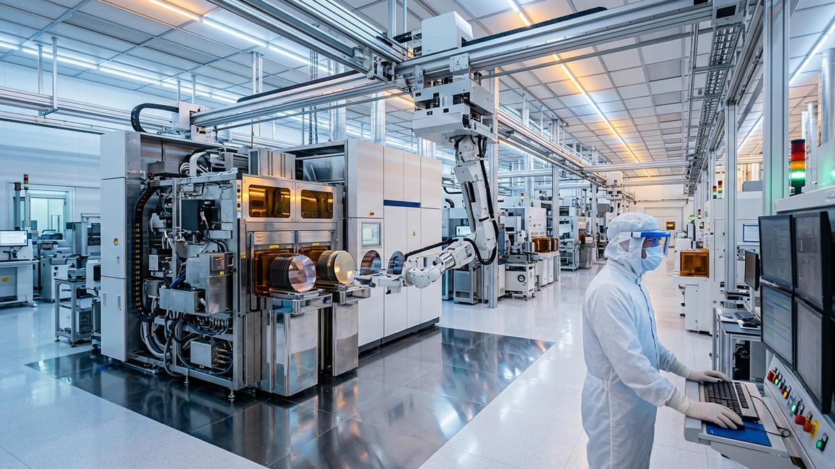
| Commercial Wafer Foundries | 28nm, 40nm, and 90nm CMOS fabrication | Tata Electronics & PSMC (Dholera, Gujarat) | Providing sovereign silicon for automotive, power, and industrial IoT applications |
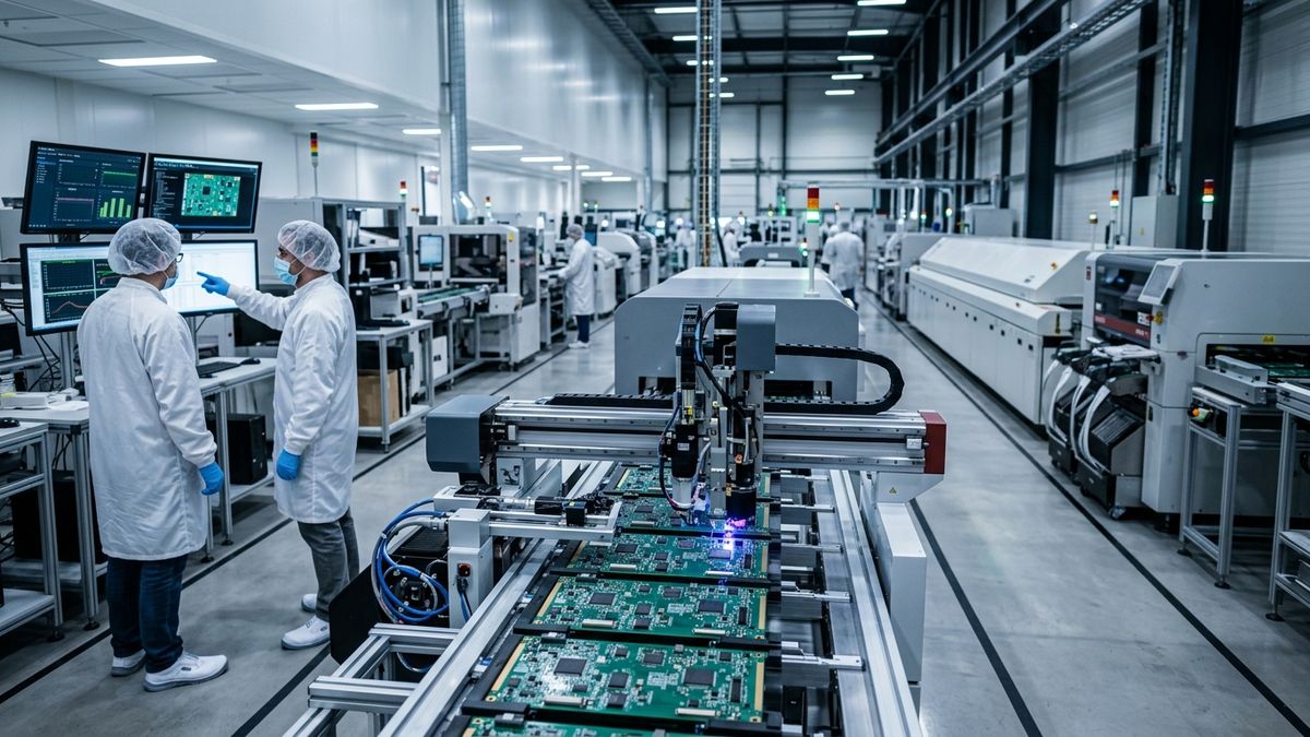
| Advanced Packaging & Testing (ATMP/OSAT) | Wire-bonding, flip-chip, 2.5D/3D system-in-package (SiP) | Micron (Sanand), Tata Electronics (Assam), CG Semi, Kaynes | Capturing rapid revenue and localizing memory module assembly within 24 months |
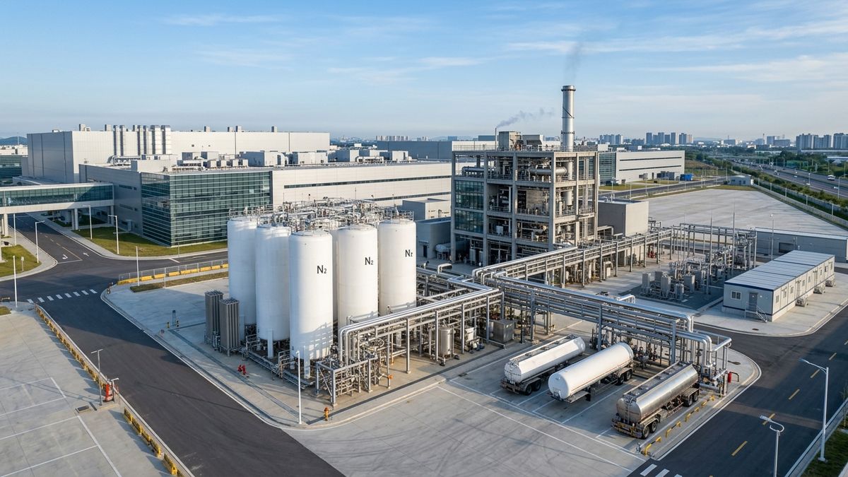
| Specialty Chemicals & Electronic Gases | Ultra-high purity (UHP) N2, Ar, O2, silane, chemical etchants | Linde expansion in Sanand, domestic chemical consortiums | Eliminating reliance on imported cryogenic specialty gases and hazardous chemicals |
| Compound Semiconductors & Photonics | Silicon Carbide (SiC) and Gallium Nitride (GaN) foundries | Domestic EV and defense compound semiconductor fabs | Powering electric vehicle powertrains, solar inverters, and high-frequency defense radar |
| Indigenous Microprocessors & HPC | RISC-V architectures, supercomputing accelerators | C-DAC (SHAKTI, VEGA cores), National Supercomputing Mission | Securing sovereign compute for defense, space, and governmental critical infrastructure |
Advanced Packaging: The Fast-Track Bridgehead
A defining revelation of SEMICON India 2026 was the strategic role played by outsourced semiconductor assembly and test (OSAT) and ATMP facilities. While building a commercial front-end wafer fabrication foundry costs upwards of $10 billion and takes 3 to 4 years to achieve full volume production, advanced packaging plants require between $500 million and $3 billion and can be operationalized within 18 to 24 months.
Micron Technology's $2.75 billion facility in Sanand serves as the pioneer, focusing on DRAM and NAND memory packaging. Concurrently, Tata Electronics' ₹27,000 crore ($3.2 billion) facility in Morigaon, Assam, and projects by CG Semi and Kaynes Technology are creating immediate industrial capacity capable of processing processed wafers into packaged chips for automotive, smartphone, and industrial clients.
Furthermore, as Moore's Law slows down, advanced 2.5D and 3D packaging technologies (chiplets) are becoming just as critical to computing performance as nanometer gate shrinking, placing packaging at the forefront of semiconductor innovation.
To see how industrial gas infrastructure is deploying directly adjacent to these packaging clusters, read our detailed report on /post/linde-expands-india-semiconductor-footprint-sanand-gujarat.
Regional Corridors: Competition Driving Execution
The progress showcased at SEMICON India reflects vigorous competitive federalism across Indian states. Gujarat has established an early lead with Dholera and Sanand, backed by plug-and-play utilities and swift land allotment. Concurrently, Uttar Pradesh has unleashed aggressive capital top-up subsidies and dedicated cleanroom utility corridors along the Yamuna Expressway (detailed in /post/up-targets-ai-semiconductors-electronics-growth), while Karnataka, Tamil Nadu, and Assam are securing significant packaging and compound semiconductor investments.
The Road to ISM 2.0
As the initial ₹76,000 crore ($10 billion) incentive corpus under ISM 1.0 approaches complete allocation across approved projects, government leadership at SEMICON India confirmed that ISM 2.0 is already in advanced drafting stages.
The next policy iteration will expand incentives to encompass semiconductor manufacturing equipment fabricators (steppers, polishers, gas cabinets), raw silicon wafer synthesis, and expanded R&D grants for fabless startups under the Design Linked Incentive (DLI) scheme.
By linking design genius with physical manufacturing execution, India is steadily securing its position as an indispensable pillar of the global semiconductor architecture.
Frequently Asked Questions
What was the central theme of SEMICON India 2026?
SEMICON India 2026 showcased the physical realization of India's semiconductor manufacturing ecosystem, highlighting how the nation is expanding beyond its traditional strength in fabless chip design into commercial foundries, advanced packaging (ATMP/OSAT), specialty chemicals, and semiconductor equipment manufacturing.
What is India's historic role in global semiconductor design?
India hosts over 20% of the global semiconductor design workforce, with more than 125,000 chip design engineers in Bengaluru, Hyderabad, and Noida working for leading multinationals like Qualcomm, Intel, Nvidia, MediaTek, AMD, and Texas Instruments.
Why is advanced packaging (ATMP/OSAT) prioritized alongside foundries?
Advanced packaging requires lower upfront capital expenditure ($500M–$3B) and shorter construction timelines (18–24 months) compared to leading-edge foundries ($10B–$20B, 3–4 years). It allows India to integrate directly into global consumer and automotive electronics supply chains while front-end fabs are under construction.
What are the key manufacturing facilities progressing under the India Semiconductor Mission?
Key approved projects include Tata Electronics' commercial fab in Dholera with Taiwan's PSMC, Micron Technology's $2.75 billion ATMP facility in Sanand, Tata Electronics' assembly and test plant in Morigaon (Assam), and OSAT plants by CG Semi and Kaynes Technology.
Primary Sources & Official References
- Ministry of Electronics and Information Technology (MeitY): India Semiconductor Mission (ISM) Annual Progress Report
- SEMI International: SEMICON India 2026 Industry Summit Proceedings & Executive Briefing
- India Electronics and Semiconductor Association (IESA): Comprehensive Semiconductor Industry Ecosystem Report
- NITI Aayog: Frontier Manufacturing & The Silicon Value Chain Strategy Paper