Lam Research Plans ₹10,000 Cr India Investment: Semiconductor Equipment Giant to Set Up Silicon Component Facility & R&D Hub
By Sanjay Patel | Published September 16, 2026 | 9 min read
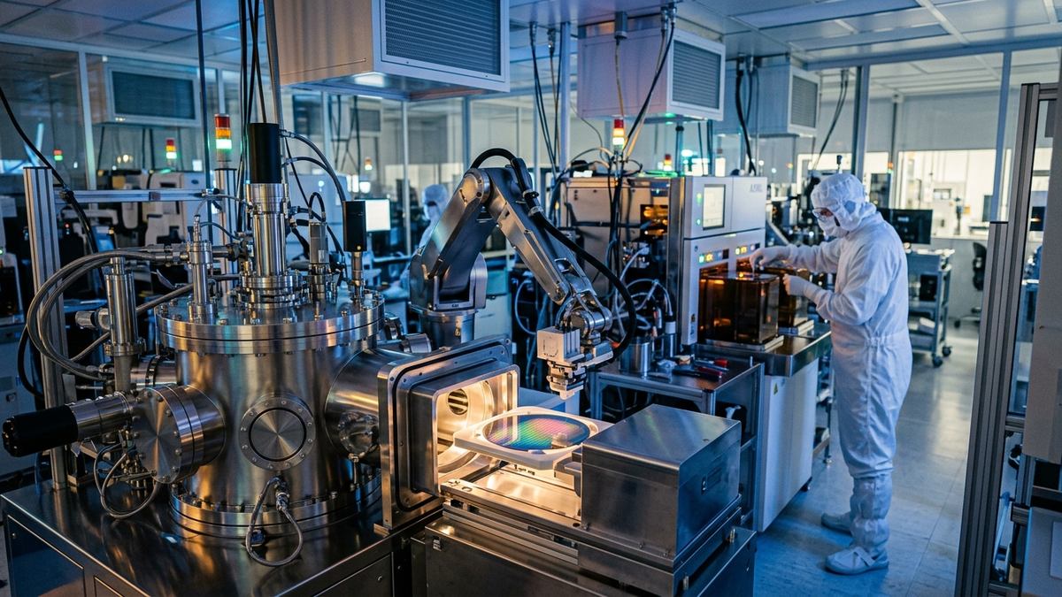
Semiconductor equipment giant Lam Research outlines a massive ₹10,000 Cr investment in India, establishing a precision silicon component facility and expanding R&D.
Global semiconductor wafer fabrication equipment (WFE) powerhouse Lam Research Corporation has detailed plans for an unprecedented ₹10,000 crore ($1.2 billion) strategic investment in India. The capital outlay will finance the establishment of a state-of-the-art silicon-component manufacturing facility, develop local precision supply chain infrastructure, and massively scale Lam’s engineering research and development (ER&D) center in Bengaluru.
The planned manufacturing plant represents a major leap for the India Semiconductor Mission (ISM). While India’s recent semiconductor milestones have largely concentrated on downstream Assembly, Testing, Marking, and Packaging (ATMP), Outsourced Semiconductor Assembly and Test (OSAT) units, and front-end commercial foundries (such as Tata Electronics' upcoming Dholera gigafab), Lam Research’s entry establishes India as a manufacturing base for the hyper-specialized equipment and silicon hardware without which no microchip fabrication facility on earth can operate.
The Critical Role of Wafer Fabrication Equipment (WFE)
Modern semiconductor fabrication is among the most scientifically demanding manufacturing processes in human history. Fabricating advanced sub-3nm node microchips requires hundreds of intricate sequential processing steps inside ultra-pure cleanroom environments.
Lam Research is one of a handful of companies globally—alongside ASML, Applied Materials, and Tokyo Electron—that possesses the proprietary physics and engineering mastery required to build wafer fabrication machinery:
* Atomic Layer Etching (ALE): Removing material with atomic-layer precision to sculpt microscopic three-dimensional transistor architectures such as Gate-All-Around (GAA) nanosheets.
* Chemical Vapor Deposition (CVD) & Atomic Layer Deposition (ALD): Depositing ultra-thin insulating and conducting films only a few angstroms thick across 300mm silicon wafers.
* High-Density Plasma Processing: Maintaining stable plasma reactions inside vacuum reaction chambers under extreme RF power densities and corrosive chemical environments.
The new ₹10,000 crore Indian facility will manufacture precision silicon and quartz components, high-purity fluid and gas delivery modules, and vacuum chamber sub-assemblies utilized inside Lam's flagship etch and deposition platforms worldwide.
"A resilient global semiconductor supply chain requires geographical diversification of precision manufacturing nodes,"noted semiconductor industry analysts during the investment announcement. "India has already demonstrated world-class chip design acumen. By anchoring physical wafer fabrication equipment and precision silicon component manufacturing in India, Lam Research is establishing the foundational hardware bedrock necessary to sustain India’s domestic fabs and global semiconductor exports."
From Virtual Cleanrooms to Physical Manufacturing
Lam Research has actively engaged with India’s semiconductor policy for several years through its Semiverse Solutions platform. In partnership with the Ministry of Electronics and Information Technology (MeitY) and leading Indian universities, Lam deployed virtual cleanroom simulation software to train over 60,000 Indian engineers in the physics of semiconductor fabrication without requiring multi-billion-dollar cleanroom operational overhead.
The transition from software-based cleanroom simulation to physical manufacturing of silicon parts reflects Lam’s escalating confidence in India's engineering talent and industrial ecosystem:
* Precision Engineering Ecosystem: Building Tier-1, Tier-2, and Tier-3 supplier clusters capable of meeting semiconductor-grade tolerances measured in nanometers and microns.
* Materials Science & Metallurgy: Qualifying domestic metallurgy, specialty ceramics, and high-purity silicon suppliers to meet stringent cleanroom contamination standards.
* Post-Silicon Testing & Metrology Integration: Seamlessly validating precision components against extreme thermal cycling, chemical corrosion, and vacuum integrity benchmarks.
This high-precision hardware commitment directly complements the testing and automated verification frameworks detailed in our investigation into Teradyne expanding its automated semiconductor test presence in Bengaluru, as well as national initiatives such as the West Bengal Quantum Technology and Semiconductor Innovation Hub at CSIR-CGCRI.
Phased Capital Allocation: Lam Research ₹10,000 Cr Investment
The table below outlines the strategic allocation, operational focus, and expected outputs across the multi-phase investment:
| Investment Phase | Capital Deployment | Operational Focus & Core Infrastructure | Strategic Target & Economic Impact |
|---|---|---|---|
| Phase 1: Precision Assembly Hub | ₹3,200 Cr | Precision machining, cleanroom sub-assembly, gas/fluid delivery integration | Supplies sub-assemblies to global Lam fabrication platforms |
| Phase 2: Silicon & Quartz Processing | ₹3,800 Cr | Dedicated silicon component cutting, polishing, and chemical passivation facility | Domestic supply of critical consumable parts for 300mm fabs |
| Phase 3: Bengaluru R&D Expansion | ₹1,800 Cr | Advanced process chemistry, computational physics modeling & hardware-in-the-loop | Accelerates 2nm and sub-2nm etch/deposition innovation |
| Phase 4: Supplier Cluster Development | ₹1,200 Cr | Qualification and incubation of domestic precision engineering vendors | Deepens indigenous semiconductor supply chain self-reliance |
Geopolitical Resilience in the Global Chip Ecosystem
The global semiconductor landscape has been repeatedly disrupted by geopolitical tensions, regional conflicts, and concentrated supply bottlenecks. Leading chipmakers across the United States, Europe, Taiwan, South Korea, and Japan are aggressively seeking diversified suppliers for both chip manufacturing and equipment sub-systems.
By committing ₹10,000 crore to Indian manufacturing, Lam Research reinforces the broader Indo-Pacific semiconductor corridor. The facility will not only supply components directly to emerging Indian chip fabrication facilities—such as Tata's Dholera plant and upcoming compound semiconductor foundries—but will also export high-value precision hardware to Lam's assembly factories across North America, Europe, and Southeast Asia.
Catalyzing India’s Deeptech Manufacturing Era
Lam Research’s ₹10,000 crore investment marks a turning point in India’s industrial evolution. It proves that India’s semiconductor ambitions are moving far beyond assembly and testing into the highest-precision equipment tier. As precision machining shops, vacuum system engineers, and materials scientists integrate into Lam’s global supply chain, India takes a decisive step toward becoming an indispensable node in the world’s semiconductor hardware architecture.