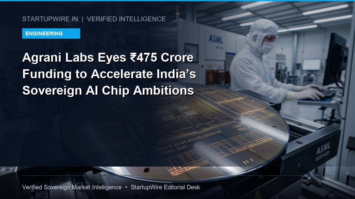
Indian Semiconductor Startups Raise $61.9 Million in H1 2026 as Ecosystem Expands Beyond Design into Packaging and AI Chips
By Rohan Varma | Published August 13, 2026 | 7 min read
India’s semiconductor startups secured $61.9M in H1 2026, marking a shift beyond fabless chip design into OSAT packaging, photonics, and AI hardware.
India’s semiconductor ecosystem witnessed a record institutional capital surge in the first half of 2026, with early-stage chip startups securing $61.9 million across 14 deals. Data compiled by industry analysts confirms a fundamental structural shift in India’s hardware landscape: venture capital is expanding rapidly beyond traditional fabless IC design into OSAT (Outsourced Semiconductor Assembly and Test) packaging, photonic integrated circuits, semiconductor equipment manufacturing, and custom AI silicon architectures.
Supported by the government's flagship India Semiconductor Mission (ISM) and matching capital incentives, Indian silicon ventures are securing international co-investments to solve sovereign compute bottlenecks and build domestic supply chain resilience.
Sector Breakdown: Capital Allocation Across Semiconductor Verticals
Unlike previous investment cycles dominated exclusively by software design tools and frontend verification, H1 2026 funding was distributed across physical hardware fabrication, advanced packaging packaging substrate manufacturing, and specialized hardware accelerators.
"India is transitioning from being the back-office layout design lab of global chip giants to an autonomous creator of custom silicon IP,"stated Dr. K. Radhakrishnan, Managing Director at the Semiconductor Innovation Council. "The $61.9M raised in H1 2026 demonstrates that private venture capital is comfortable underwriting hardware development timelines when backed by sovereign policy incentives and strong enterprise off-take agreements."
This capital inflow directly addresses the infrastructure imperatives discussed in our deep-dive on India’s sovereign AI compute bottleneck, while complementing industrial breakthroughs like Gujarat's RISC-V IoT chip initiatives.
H1 2026 Indian Semiconductor Funding Breakdown
The matrix below illustrates the allocation of the $61.9 million raised by Indian semiconductor startups during the first six months of 2026:
| Semiconductor Sub-Sector | Total Capital Raised (H1 2026) | Deal Count | Core Strategic Deliverable | Key Technology Stack |
|---|---|---|---|---|
| Fabless Chip Design | $24.8 Million | 5 Deals | Edge AI Accelerators & RISC-V Microcontrollers | 28nm / 12nm RISC-V Silicon |
| OSAT & Advanced Packaging | $18.5 Million | 3 Deals | 2.5D/3D Chiplet Assembly & Substrates | Heterogeneous Packaging |
| Silicon Photonics & Optical Interconnects | $9.2 Million | 2 Deals | High-Bandwidth Data Center Interconnects | Indium Phosphide Photonics |
| Semiconductor Equipment & Fab Tooling | $5.8 Million | 2 Deals | Automated Wafer Inspection & Precision Optics | Computer Vision Inspection |
| Power Semiconductors (GaN/SiC) | $3.6 Million | 2 Deals | EV Inverters & Industrial Power Modules | Gallium Nitride (GaN) Tech |
RISC-V and Edge AI Lead Fabless Investments
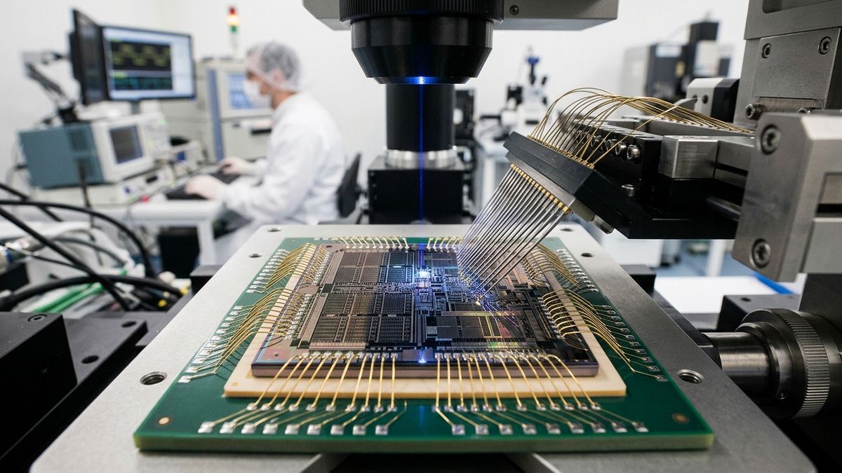
Fabless startups captured the largest single share of funding ($24.8M), driven by intense demand for domain-specific AI hardware. Indian fabless teams are designing specialized RISC-V accelerator cores tailored for computer vision in smart industrial automation, autonomous mobility, and defense electronics.
By leveraging open-standard RISC-V instruction sets, Indian startups avoid costly proprietary architecture licensing fees, allowing them to allocate more capital toward physical tape-outs and sample production at foundry partners in Taiwan, South Korea, and domestic pilot facilities.
Rise of OSAT and Micro-Packaging Hubs
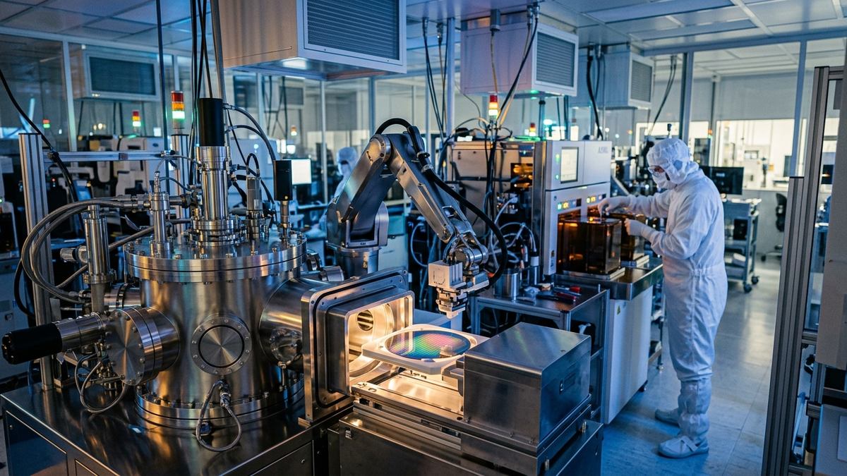
A standout trend in H1 2026 is the emergence of specialized OSAT and advanced micro-packaging ventures. With global chipmakers shifting toward chiplet-based architectures, packaging has become as critical as transistor scaling. Indian packaging startups are building pilot lines for 2.5D substrate assembly and thermal dissipation testing in Bengaluru, Hyderabad, and Dholera.
These packaging ventures provide crucial testing grounds for domestic fabless chipmakers, shortening prototyping cycles from months to weeks and establishing a self-sustaining hardware ecosystem within India.