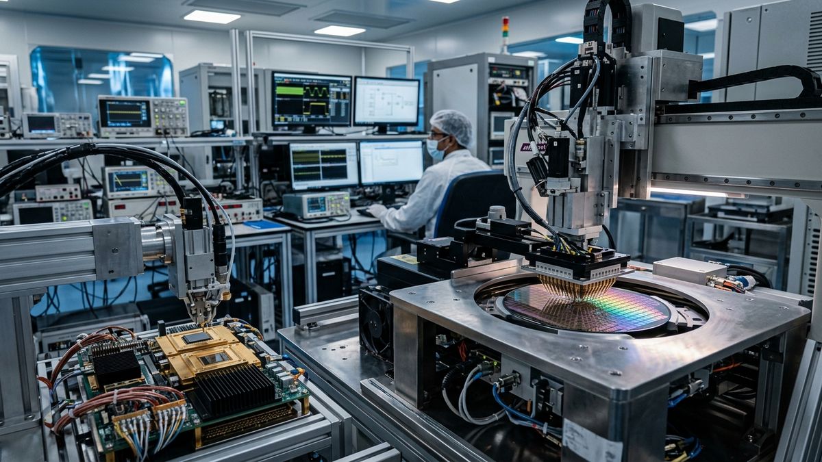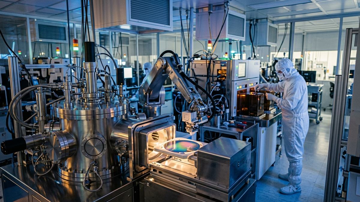
Bengaluru deeptech fabless startup Agrani Labs is seeking ₹475 crore in major funding to accelerate tape-outs, silicon validation, and engineering for domestic AI accelerators.
Executive Key Takeaways
- Bengaluru deeptech fabless startup Agrani Labs is seeking ₹475 crore in major funding to accelerate tape-outs, silicon validation, and engineering for domestic AI accelerators.
- India cannot remain purely a consumer of imported computing silicon if it intends to establish sovereign AI autonomy, noted senior semiconductor architects tracking the round. Agrani Labs' targeted approach toward tape-out execution demonstrates that domestic engineering talent is moving up the value chain from physical design services to full-architecture product ownership.
- Key Benchmark: **Primary Workload Target** — LLM Inference & Dynamic Sparsity
BENGALURU — In what marks a decisive escalation in India’s quest for silicon sovereignty, Bengaluru-based deeptech startup Agrani Labs is in advanced discussions to raise ₹475 crore ($57 million) in fresh equity funding to accelerate research, tape-outs, and commercial fabrication of specialized artificial intelligence (AI) microchips.
The capital infusion will fund silicon prototyping, multi-project wafer (MPW) runs at leading global semiconductor foundries, software-stack compiler development, and high-frequency hardware emulation rigs. As global technology powers race to secure proprietary compute architectures, Agrani Labs aims to position India as a credible designer of energy-efficient, application-specific integrated circuits (ASICs) tailored for transformer models, edge vision inference, and hyperscale neural network workloads.
This funding push follows a broader renaissance across India's microelectronics landscape, echoing developments analyzed in Infineon Acquires Bengaluru Chip Startup C2i Semiconductors and the human-capital ramp profiled in Semicon 2.0 Targets 1 Lakh Semiconductor Engineers.
Architectural Focus: Tailoring Silicon for Generative AI and Edge Workloads
Traditional general-purpose graphics processing units (GPUs) remain notoriously power-hungry and capital-intensive, presenting prohibitive cost bottlenecks for domestic enterprises seeking to deploy localized LLMs. Agrani Labs' engineering philosophy centers on domain-specific architecture (DSA)—stripping away legacy graphics rendering pipelines to dedicate die area entirely to matrix-multiplication acceleration, high-bandwidth memory (HBM) interconnects, and dynamic sparsity handling.
Agrani’s proprietary neural processing unit (NPU) architecture integrates:
1. Massive Matrix Math Units (MMUs): Custom systolic array cores engineered to maximize FP8 and INT4 inference throughput while slashing thermal dissipation.
2. SRAM-Dense Near-Memory Compute: Minimizing the high energy penalty of off-chip data transfers by keeping model weights in dense on-chip cache.
3. Unified Compiler Ecosystem: An open-standard runtime compiling directly from PyTorch, JAX, and ONNX into bare-metal machine code, reducing software dependency on proprietary stacks.
"India cannot remain purely a consumer of imported computing silicon if it intends to establish sovereign AI autonomy,"noted senior semiconductor architects tracking the round. "Agrani Labs' targeted approach toward tape-out execution demonstrates that domestic engineering talent is moving up the value chain from physical design services to full-architecture product ownership."
Technical & Operational Benchmark: Agrani Silicon Roadmap vs. Industry Standards
The comparison matrix below outlines Agrani Labs' projected silicon parameters alongside prevailing enterprise accelerator benchmarks:
| Parameter / Metric | Agrani Labs (Projected NPU) | Enterprise GPU Standard | Commercial Edge TPU |
|---|---|---|---|
| Primary Workload Target | LLM Inference & Dynamic Sparsity | Universal Training & HPC | Micro Edge Vision & Sensor Fusion |
| Target Process Node | 4nm / 5nm Advanced FinFET | 3nm / 4nm Leading Node | 12nm / 16nm Mature Node |
| Target Energy Efficiency | 18–24 TOPS / Watt (FP8) | 8–12 TOPS / Watt | 14–16 TOPS / Watt (INT8) |
| Interconnect Architecture | Open-Standard Chiplet UCIe | Proprietary High-Speed Bus | PCIe Gen 4/5 Standard |
| Compiler Stack | Native PyTorch/Triton Integration | Proprietary Closed Ecosystem | Model Quantization Toolkits |
Policy Tailwinds: Leveraging the India Semiconductor Mission (ISM)
Agrani Labs’ funding initiative intersects with government incentives under the India Semiconductor Mission (ISM) and the Design-Linked Incentive (DLI) Scheme. The Ministry of Electronics and Information Technology (MeitY) has earmarked substantial financial reimbursement packages covering up to 50% of eligible design and tape-out expenditures for indigenous fabless ventures.
By combining private venture capital with government matching grants, Agrani Labs plans to de-risk the prohibitively expensive tape-out cycle—where a single 5nm photomask set can demand upwards of $15 million. This blended finance model mirrors successful state-backed chip ecosystems in Taiwan, South Korea, and the United States, as detailed in our analysis on India's Deeptech Ecosystem Gains Policy and Funding Momentum.
Market Outlook: From Bengaluru Design Centers to Commercial Data Centers
Agrani Labs expects to finalize the ₹475 crore equity syndicate within the coming months, with participation anticipated from sovereign-backed deeptech funds, domestic institutional investors, and strategic cloud operators. First-silicon engineering samples are scheduled for packaging and laboratory testing by late 2026, with pilot server blade deployments slated for Indian sovereign data centers by mid-2027.
If successfully realized, Agrani Labs' breakthrough will mark a historic transition for India’s semiconductor ecosystem: graduating from an offshore design hub that drafts circuits for foreign tech giants into an autonomous creator of world-class silicon intellectual property.