India’s Semiconductor Ecosystem Moves Toward Scale: 200 Chip-Design Target and Mass EDA Access for 105 Startups
By Sanjay Patel | Published September 20, 2026 | 8 min read
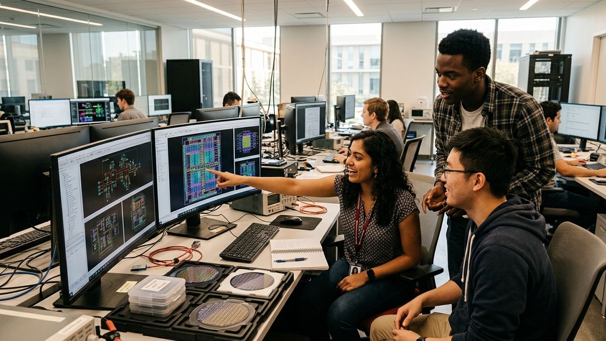
India targets 200 indigenous chip-design ventures as MeitY equips 105 fabless startups and 400 engineering colleges with cloud-hosted, enterprise-grade EDA software suites.
India’s strategic ambition to become a global microelectronics powerhouse has shifted into high gear, as the central government established a definitive target of scaling 200 indigenous chip-design companies while democratizing access to electronic design automation (EDA) software across 105 startups and 400 engineering universities. Spearheaded by the Ministry of Electronics and Information Technology (MeitY) and the India Semiconductor Mission (ISM), the initiative dismantles the single highest barrier to entry in the semiconductor sector: multi-million-dollar software tool licensing and physical silicon prototyping costs.
By democratizing access through centralized cloud infrastructure, India is transforming its massive workforce of VLSI engineers—who historically designed intellectual property for multinational corporations—into founders of homegrown fabless enterprises building proprietary silicon products for telecom, automotive, defense, and AI edge computing.
The Prohibitive Barrier of Semiconductor Design Economics
Building a commercial fabless semiconductor company requires steep upfront capital long before the first working silicon die is ever taped out. A standard 16nm or 7nm design requires:
- EDA Software Licenses: Enterprise tool suites for schematic capture, synthesis, place-and-route, physical verification, and electromagnetic simulation from Synopsys, Cadence, and Siemens EDA run between $200,000 and $500,000 per seat annually.
- PDK and IP Core Access: Foundry-specific Process Design Kits (PDKs) and third-party interface IP (PCIe, DDR5, USB-4) demand substantial upfront commitment fees.
- Tape-Out Shuttle Costs: Submitting a test chip to an international foundry shuttle via Multi-Project Wafer (MPW) runs costs $100,000 to $500,000 per iteration.
Historically, this financial bottleneck restricted domestic innovation to well-capitalized multinational subsidiaries in Bengaluru and Hyderabad, effectively shutting out student innovators and early-stage entrepreneurs.
"A country that aspires to lead the digital age cannot merely assemble foreign circuit boards—it must invent the silicon logic that directs them,"stated MeitY officials during an ecosystem briefing. "By democratizing EDA suites and funding tape-outs, we are creating a fertile runway for 200 world-class Indian chip startups."
This democratization directly complements breakthroughs like Chennai startup Aheesa Digital unveiling the Vihaan-I RISC-V broadband processor and aligns with Intel's assessment that 20% of the world's silicon design workforce is powered by Indian engineers.
Centralized Cloud Infrastructure: The C-DAC ChipIN Centre
To execute this massive democratization, MeitY established the ChipIN Centre hosted at C-DAC Bangalore. The facility acts as a digital semiconductor foundry, delivering centralized virtual desktop infrastructure (VDI) equipped with the entire spectrum of cutting-edge EDA tools:
| Component | Target Coverage | Tooling / Infrastructure Provided | Strategic Impact |
|---|---|---|---|
| Startup Incubation | 105 Fabless Startups | Cadence, Synopsys, Siemens EDA cloud licenses | Zero upfront software licensing expenditure |
| Academic Institutions | 400 Engineering Colleges | Centralized VLSI lab workstations & verified PDKs | 85,000 industry-ready VLSI graduates by 2028 |
| Design-Linked Incentive | Up to 50% Fiscal Support | Product development reimbursement & MPW funding | De-risked physical tape-out iterations |
| Silicon Tape-Out Shuttles | MPW Access via SCL & TSMC | Silicon validation for multi-core RISC-V & analog ICs | Faster time-to-market for production chips |
Nurturing Sovereign IP in Automotive, IoT, and AI Edge
With over 105 startups already on-boarded to the ChipIN platform, domestic innovators are targeting high-growth semiconductor niches where agility and domain-specific architectures provide competitive advantages:
- Automotive Power Management: Custom battery management ICs (BMS) and motor controller gate drivers optimized for electric two-wheelers operating in extreme thermal environments.
- Industrial IoT & Edge Computing: Low-power sensor fusion chips with embedded machine learning micro-cores for predictive vibration analysis in smart manufacturing plants.
- Telecom & Optical Networking: High-speed serializer/deserializer (SerDes) silicon and optical transceiver ICs designed to replace imported networking hardware.
Academic Modernization: From Theory to Real Silicon
Crucially, the government’s target of 200 chip-design companies is underpinned by comprehensive talent pipelines. Through the Chips to Startup (C2S) initiative, 400 engineering colleges—including national IITs, NITs, and regional technical universities—have discarded legacy synthetic circuit simulations in favor of actual multi-project wafer tape-outs.
Students now write Verilog/SystemVerilog RTL code, perform timing closure and design rule checking (DRC) against genuine foundry PDKs, and receive physical silicon test chips back from fabrication facilities. This hands-on physical design expertise eliminates the multi-year retraining periods previously required when hiring university graduates into commercial semiconductor labs.
Strategic Outlook: From Design Services to Sovereign Silicon Brands
As India’s hardware ecosystem matures, the transition from offshore design captives to domestic IP ownership represents a permanent structural transformation. With 105 startups actively designing, 400 colleges supplying a stream of verified talent, and national foundries taking shape in Sanand and Dholera, the roadmap toward 200 domestic fabless enterprises is establishing an enduring foundation for India's technological independence.
Frequently Asked Questions
What is the government's target for domestic chip-design ventures?
Under the India Semiconductor Mission, the central government has set a target to nurture, incubate, and scale 200 indigenous fabless chip-design enterprises by 2028.
How are 105 startups and 400 engineering colleges gaining access to EDA tools?
MeitY and the C-DAC ChipIN Centre provide centralized, secure cloud-hosted access to industry-grade EDA tools from Synopsys, Cadence, and Siemens EDA, subsidizing software licenses that normally cost hundreds of thousands of dollars.
What is the role of the C-DAC ChipIN Centre?
The ChipIN Centre serves as a centralized semiconductor design infrastructure portal offering EDA tool licenses, design rule checks (DRC), virtual silicon prototyping, and subsidized multi-project wafer (MPW) fabrication access.
Which chip architectures are Indian startups developing?
Indian fabless startups are developing custom RISC-V edge processors, AI/NPU accelerators, automotive microcontrollers, power management ICs (PMICs), and 5G RF front-end chips.
Primary Sources & Official References
- Ministry of Electronics and Information Technology (MeitY): ChipIN Centre Annual Operations Report: Statistical documentation of tools and startup onboarding.
- Centre for Development of Advanced Computing (C-DAC): Chips to Startup (C2S) Infrastructure Brief: Guidelines on academic VLSI modernization.
- India Semiconductor Mission: Design-Linked Incentive (DLI) Guidelines & Allocation Metrics: Official fiscal support benchmarks for fabless ventures.
- India Electronics and Semiconductor Association (IESA): Fabless Ecosystem Scaling Analysis: Empirical industry whitepaper on domestic semiconductor startups.