Intel Highlights India’s Semiconductor Talent: 20% of Global Chip-Design Workforce Powered by Indian Engineers
By Sanjay Patel | Published September 18, 2026 | 8 min read
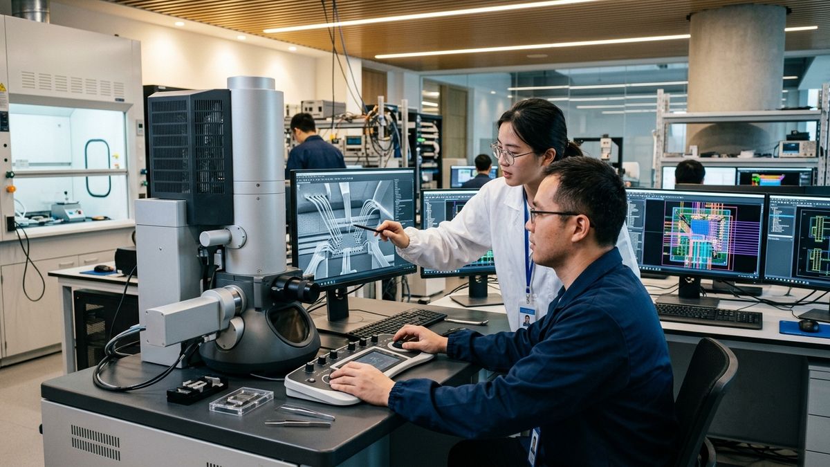
Intel spotlights India’s dominance in global silicon design, contributing 20% of chip-design engineers supported by over 100 university VLSI programmes.
Global semiconductor pioneer Intel has highlighted India’s commanding position in the international microelectronics landscape, revealing that the country already contributes approximately 20 percent of the world’s chip-design and silicon verification workforce. Backed by a vast academic pipeline of hundreds of engineering colleges offering accredited Very Large Scale Integration (VLSI), microelectronics, and electronic system design programmes, India is rapidly moving beyond physical layout verification to architecting core microprocessor intellectual property (IP), custom AI accelerators, and complex System-on-Chip (SoC) architectures.
For over two decades, multinational semiconductor leaders—including Intel, AMD, Nvidia, Qualcomm, Broadcom, and Texas Instruments—have maintained extensive research and development centres in Bengaluru and Hyderabad. However, the depth and architectural autonomy of India's silicon design talent has reached an unprecedented inflection point, driven by national policy support under the India Semiconductor Mission (ISM) and the Ministry of Electronics and Information Technology (MeitY).
The Intellectual Engine: From Layout Routing to Core Microarchitecture
In the early 2000s, semiconductor operations in India primarily handled post-silicon physical design, standard cell placement, and timing closure for designs conceived in Santa Clara or Austin. Today, Indian design centres spearhead end-to-end silicon lifecycles:
* Microarchitecture Specification: Defining register-transfer level (RTL) logic, instruction fetch pipelines, branch prediction algorithms, and out-of-order execution engines for enterprise server processors.
* Silicon Verification & Emulation: Writing complex Universal Verification Methodology (UVM) testbenches and running hardware emulators (such as Cadence Palladium and Synopsys ZeBu) to validate billions of logic gates before tape-out.
* AI & Neuromorphic Acceleration: Engineering specialized matrix multiplication units, tensor cores, and low-precision INT4/FP8 compute pipelines integrated into client and data centre processors.
* Mixed-Signal and High-Speed SerDes: Designing ultra-high-speed PCIe Gen 6, CXL, and LPDDR5X physical interfaces (PHY) critical for high-bandwidth server connectivity.
"India is already the silicon brain of the global technology sector,"emphasized senior semiconductor engineering leadership. "One out of every five chip-design engineers worldwide is based in India. With our engineering institutions now equipping tens of thousands of students with industry-grade EDA tools each year, India has a golden opportunity to convert this talent base into indigenous fabless chip powerhouses."
Academic Grounding: The "Chips to Startup" (C2S) Revolution
A crucial factor behind this talent explosion is the central government’s Chips to Startup (C2S) programme, which aims to train 85,000 specialized semiconductor engineers across 100+ universities, IITs, and NITs over a five-year horizon.
Under C2S, academic labs receive:
1. Centralized Electronic Design Automation (EDA) Tool Access: State-of-the-art software suites from Synopsys, Cadence, and Siemens EDA hosted on centralized cloud servers, eliminating multi-million-dollar licensing barriers for educational institutions.
2. Multi-Project Wafer (MPW) Tape-Out Grants: Enabling student engineering teams and PhD scholars to submit integrated circuit designs for real silicon tape-out at commercial foundries (such as TSMC, GlobalFoundries, or SCL Mohali).
3. Curriculum Modernization: Updating electronics engineering syllabi to include RISC-V processor design, hardware description languages (SystemVerilog, Chisel), and advanced physical packaging design rules.
This academic-industry convergence mirrors groundbreaking research hubs across the country, such as the West Bengal Quantum & Semiconductor Innovation Hub at CSIR-CGCRI Kolkata and precision tooling pivots detailed in our analysis of Indian engineering manufacturers expanding into semiconductor tooling.
Talent & Infrastructure Matrix: India’s Semiconductor Ecosystem
The table below outlines the core dimensions of India's chip-design talent pool, academic distribution, and industry footprint:
| Dimension | Current Baseline | 2028 Projection | Strategic Impact |
|---|---|---|---|
| Global Chip Design Share | ~20% of Global Engineers | ~25% – 28% Global Share | Core pillar of worldwide semiconductor IP |
| Active VLSI Engineers | 125,000+ Specialists | 210,000+ Specialists | World's fastest-growing silicon engineering pool |
| Universities with EDA Access | 120+ Institutions | 300+ Engineering Colleges | Broad democratisation of hardware design |
| Indigenous Fabless Startups | ~65 Startups | 200+ Fabless Ventures | Evolution from services to domestic chip IP |
| Annual Real Tape-Outs (MPW) | 45 Academic Chips | 180+ Silicon Tape-Outs | Real silicon debugging experience for graduates |
Transitioning from Design Captives to Sovereign Fabless Startups
While multinational captives continue to hire aggressively, the most exciting frontier of India’s semiconductor talent boom is the birth of homegrown fabless startups. Ventures such as VerifAIX, which secured $5M for AI-powered chip verification, and RISC-V pioneers are capitalizing on this experienced engineering pool to build proprietary IP.
Furthermore, as physical packaging hubs ramp up operations—exemplified by Micron scaling up its Sanand ATMP facility—Indian chip architects will finally be able to verify, package, and test their indigenous silicon designs entirely within domestic borders.
Future Outlook: Building the Sovereign Silicon Corridor
Intel’s affirmation of India’s 20 percent global design workforce highlights the strong foundation beneath the India Semiconductor Mission. As the nation couples its intellectual dominance in logic design with multi-billion-dollar physical fabs and OSAT packaging lines, India is cementing its role as a permanent, indispensable superpower in the global microelectronics architecture.