Linde Expands India Semiconductor Footprint with Sanand Land Acquisition: Bolstering Ultra-High Purity Gases for Gujarat Chip Cluster
By Sanjay Patel | Published September 29, 2026 | 8 min read
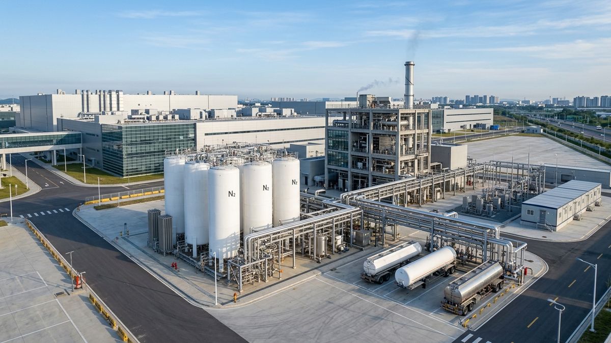
Industrial gas major Linde acquires strategic land in Sanand, Gujarat, establishing dedicated ultra-high-purity gas infrastructure for India's emerging semiconductor manufacturing corridor.
Industrial gas giant Linde has completed the acquisition of a prime industrial land parcel in Sanand, Gujarat, formalizing plans to establish an advanced production and pipeline distribution facility for ultra-high-purity (UHP) electronic specialty gases. The strategic investment directly addresses one of the most demanding operational prerequisites for commercial chipmaking, embedding critical auxiliary infrastructure adjacent to India's fastest-growing semiconductor assembly, testing, marking, and packaging (ATMP) corridor.
The development represents a vital milestone for the India Semiconductor Mission (ISM). While public discourse frequently focuses on multi-billion-dollar wafer fabrication foundries and outsourced semiconductor assembly and test (OSAT) plants, microelectronics manufacturing cannot function without continuous, localized access to electronic-grade specialty chemicals and cryogenic gases delivered at institutional purity thresholds.
By anchoring dedicated supply capabilities within Sanand, Linde is positioning itself as the foundational industrial gas backbone for both anchor tenants like Micron Technology and subsequent waves of compound semiconductor and packaging players setting up operations across Gujarat.
The Chemistry of Silicon: Why Gas Purity Dictates Fab Yields
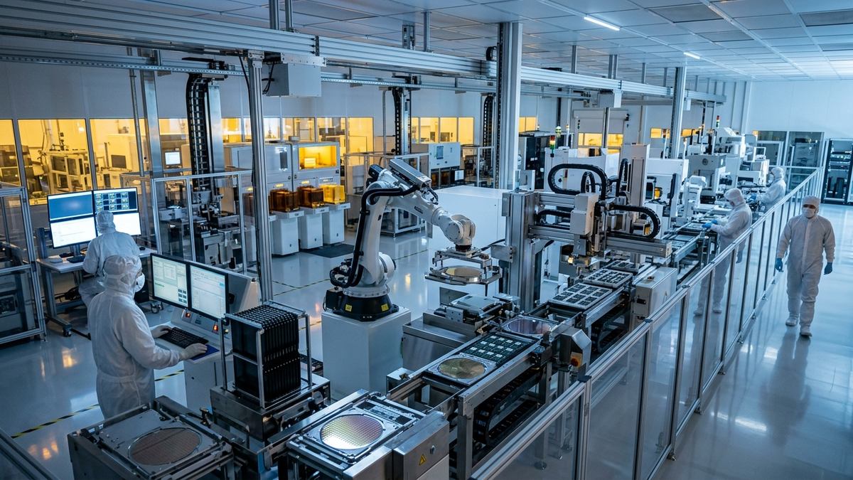
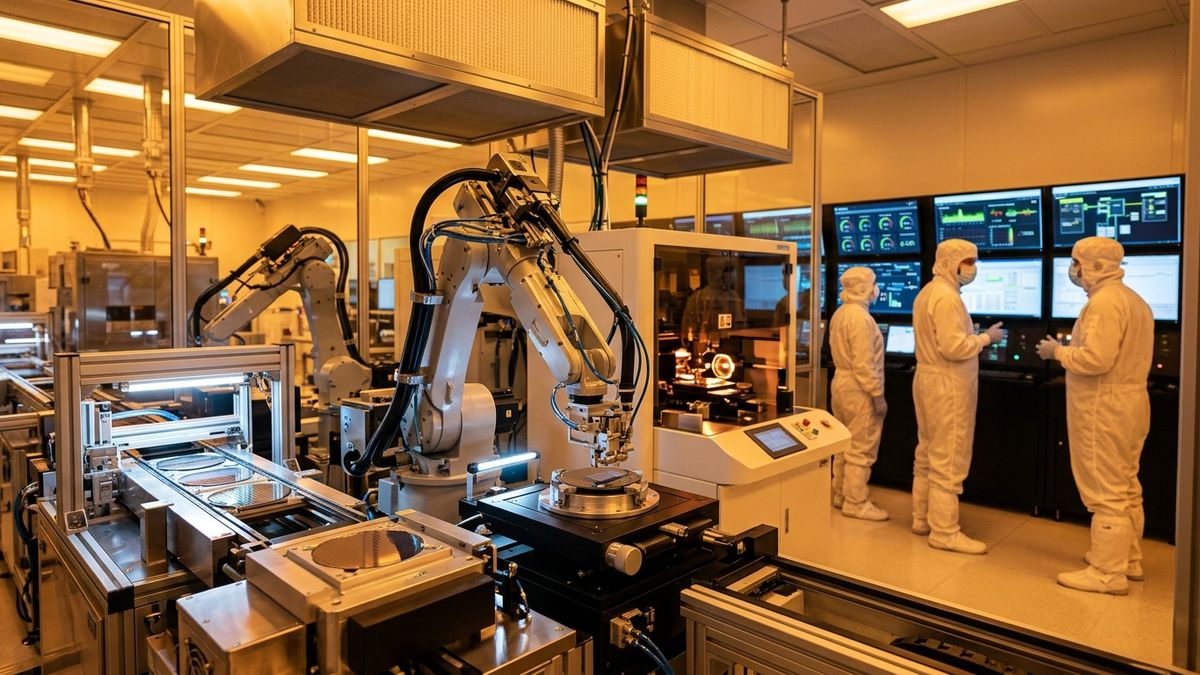
In modern microelectronics manufacturing, industrial gases are not incidental consumables; they are reactive chemical agents and inert protective shields that directly dictate semiconductor yields. During front-end wafer fabrication and back-end advanced packaging, silicon substrates undergo hundreds of sequential chemical, thermal, and mechanical cycles.
Photolithography, reactive ion etching, chemical vapor deposition (CVD), and atomic layer deposition (ALD) require continuous streams of specialty and bulk gases. Any foreign particulate matter, trace moisture, or hydrocarbon contamination measured in parts-per-billion (ppb) or parts-per-trillion (ppt) can corrupt circuit geometries measuring mere nanometers in width, rendering entire silicon wafers defective.
To sustain commercial operations, semiconductor facilities require ultra-high-purity (UHP) grades of at least 99.9999% (known in the industry as 6N purity) or 99.99999% (7N purity). Transporting these specialized cryogenic liquids across international borders incurs prohibitive logistics costs and elevated contamination risks, making localized production facilities essential.
"A semiconductor cleanroom is only as reliable as the molecular integrity of the gases pumped into its reaction chambers,"noted a senior chemical engineering specialist advising the India Semiconductor Mission. "Establishing an on-site or adjacent electronic gas synthesis and purification plant transforms a regional industrial park into an authentic, self-sustaining microelectronics ecosystem."
Critical Gases in the Semiconductor Supply Chain
Linde's Sanand infrastructure is designed to process, purify, and distribute both bulk atmospheric gases and high-value electronic specialty gases (ESGs) tailored to packaging and foundry specifications:
| Gas Classification | Chemical Formula | Process Application in Chipmaking | Typical Required Purity |
|---|---|---|---|
| Electronic Nitrogen | N2 | Inert carrier gas, purge cycles, cleanroom atmospheric control | 99.9999% (6N) |
| High-Purity Argon | Ar | Plasma sputtering, inert shielding during laser dicing | 99.99995% (6.5N) |
| Ultra-Pure Oxygen | O2 | Silicon thermal oxidation, plasma ashing, oxide dielectric growth | 99.9999% (6N) |
| Electronic Hydrogen | H2 | Annealing atmospheres, epitaxial deposition carrier | 99.99999% (7N) |
| Silane | SiH4 | Silicon dioxide and silicon nitride chemical vapor deposition (CVD) | 99.9995% (5.5N) |
| Nitrogen Trifluoride | NF3 | In-situ plasma chamber cleaning, chemical reactor decontamination | 99.999% (5N) |
Sanand as the Epicenter of India's Hardware Corridor
The choice of Sanand underscores Gujarat's emerging hegemony as India's primary semiconductor testing and packaging capital. Located approximately 30 kilometers from Ahmedabad, Sanand has evolved from an automotive manufacturing cluster into a high-technology industrial node.
Micron Technology's $2.75 billion ATMP facility, which broke ground in Sanand, represents the anchor tenant driving demand for specialized local suppliers. In addition to Micron, ventures such as CG Semi and Kaynes Technology have committed capital toward assembly and testing operations in the state, while Tata Electronics is progressing on its $11 billion commercial fab in nearby Dholera in partnership with Taiwan's Powerchip Semiconductor Manufacturing Corporation (PSMC).
By locating its gas infrastructure in Sanand, Linde establishes an operational radius that can cost-effectively serve both Sanand's packaging facilities and Dholera's front-end foundry through cryogenic trailers and specialized tube trailers, creating seamless auxiliary integration across Gujarat's industrial corridor.
Readers tracking regional policy developments can explore our dedicated breakdown on /post/up-targets-ai-semiconductors-electronics-growth to understand how competing states are structuring fiscal incentives for hardware clusters.
Supply Chain Resilience and Sovereign Capabilities
Historically, India's electronics sector relied entirely on imports for electronic-grade chemicals and specialty cylinder gases, exposing domestic contract manufacturers to global supply bottlenecks and volatile shipping tariffs. The establishment of dedicated domestic purification and packaging infrastructure mitigates these vulnerabilities.
Linde's operational model incorporates cryogenic air separation units (ASUs), dedicated purification columns, analytical testing laboratories capable of continuous trace metal detection, and automated cylinder filling manifolds built to international semiconductor safety guidelines.
Furthermore, localized gas availability directly reduces the capital expenditure and operational friction for incoming international fabless design firms, OSAT operators, and compound semiconductor startups considering India as an alternative manufacturing base to Taiwan, South Korea, and China.
For an extensive perspective on institutional venture capital flowing into frontier hardware and deeptech ecosystems, see our analysis on /post/indias-deep-tech-funding-momentum-builds-space-quantum-batteries.
Long-Term Outlook for Industrial Gas Infrastructure
As the India Semiconductor Mission progresses toward its second phase (ISM 2.0), government incentives are expanding beyond primary fab anchors to encompass component suppliers, chemical manufacturers, and equipment service providers.
Linde's Sanand expansion is expected to serve as a catalyst for other specialized auxiliary suppliers, including ultra-pure water (UPW) treatment system providers, hazardous chemical abatement engineers, and specialized cleanroom HVAC fabricators. The synchronized development of these foundational support industries marks India's transition from speculative semiconductor aspirations toward enduring, globally competitive manufacturing realities.
Frequently Asked Questions
What is Linde's new investment in Sanand, Gujarat?
Linde has acquired strategic industrial land in Sanand to construct an advanced industrial and electronic gas manufacturing center designed to supply ultra-high-purity (UHP) process gases directly to the expanding Gujarat semiconductor and electronics cluster.
Why are ultra-high-purity gases critical to semiconductor fabrication?
Semiconductor manufacturing processes, including photolithography, chemical vapor deposition (CVD), etching, and packaging, require bulk and specialty gases at purities exceeding 99.9999% (6N). Even minute parts-per-billion impurities can cause critical electrical shorts or crystal defects on silicon wafers.
Which semiconductor facilities will benefit from Linde's Sanand hub?
The primary beneficiary is the Sanand semiconductor corridor, home to Micron Technology's $2.75 billion assembly and test facility, as well as multiple upcoming OSAT and ATMP ventures approved under the India Semiconductor Mission (ISM).
How does this investment fit into the broader India Semiconductor Mission?
While initial attention centered on chip foundries, a resilient semiconductor ecosystem requires localized supply chains for specialty chemicals, ultra-pure water, and electronic gases. Linde's footprint ensures that domestic chipmakers avoid fragile international cryogenic supply chains.
Primary Sources & Official References
- Linde India Regulatory Filing: Strategic Land Allocation & Specialty Industrial Gas Expansion
- Gujarat Industrial Development Corporation (GIDC): Sanand Semiconductor Industrial Park Allotment Registry
- India Semiconductor Mission (ISM): Electronic Materials and Auxiliary Chemicals Infrastructure Roadmap
- SEMI International: Global Standards for Electronic Grade Specialty Gases and Wafer Fabrication Materials