UP Targets AI, Semiconductors & Electronics Growth: Building India’s Northern Hardware Corridor
By Sanjay Patel | Published September 28, 2026 | 8 min read

Uttar Pradesh unleashes aggressive capital subsidies, 24/7 dedicated clean power, and Yamuna Expressway land corridors to establish a major semiconductor and AI electronics hub.
Uttar Pradesh is executing an aggressive industrial pivot to establish itself as India's premier northern semiconductor, artificial intelligence infrastructure, and advanced electronics manufacturing bastion. Backed by sweeping fiscal incentives, dedicated 24/7 power substations, and contiguous land allocations along the Yamuna Expressway, the state government is positioning its industrial corridors to capture multi-billion-dollar investments in semiconductor fabrication, outsourced assembly and testing (OSAT), and enterprise AI electronics.
Having already captured over 60% of India's mobile phone manufacturing footprint through major facilities in Noida and Greater Noida, Uttar Pradesh is now systematically moving up the global value chain from simple consumer electronics assembly to capital-intensive silicon fabrication and automated hardware engineering.
The Strategic Policy Arsenal: Top-Up Subsidies and Land Concessions
At the center of Uttar Pradesh's manufacturing offensive is its dedicated Semiconductor Policy 2024–2029. The framework was specifically engineered to harmonize with the Central Government's ₹76,000 crore India Semiconductor Mission (ISM), providing one of the most lucrative incentive packages in the Indo-Pacific region:
- Capital Expenditure Top-Up: The state provides a 50% top-up subsidy on the capital assistance granted by the Central Government, effectively covering up to 75% of total fab project costs in combined sovereign incentives.
- Land Acquisition Rebates: The Yamuna Expressway Industrial Development Authority (YEIDA) offers a 75% subsidy on prevailing land rates for the first 200 acres acquired for primary wafer fabs and packaging facilities.
- Power and Water Subsidies: Chip fabrication demands unyielding stability; a split-second power outage can ruin an entire silicon wafer production batch. UP guarantees zero-interruption dual-grid feeds from dedicated 400kV and 220kV substations, coupled with 10-year electricity duty exemptions and subsidized tariff rates.
- Complete Stamp Duty Waiver: 100% exemption on stamp duty and registration fees on land purchases and lease deeds for semiconductor units.
"Silicon and AI infrastructure require structural certainty above all else,"emphasized a senior state industrial policymaker. "By combining contiguous land banks directly adjacent to an international cargo airport with guaranteed ultra-pure water and uninterrupted power, Uttar Pradesh is removing the historic operational friction that once diverted microelectronics investments to Southeast Asia."
This ambitious state roadmap dovetails with national supply chain expansions detailed in India's semiconductor push creating new supply-chain opportunities, where ancillary materials and testing ecosystems are localizing at record speeds.
The Yamuna Expressway Tech Corridor: Infrastructure Built for Atoms
The anchor of UP's microelectronics ambition is the planned Semiconductor Park in Sector 10 and Sector 28 under YEIDA, located less than 10 kilometers from the upcoming Noida International Airport at Jewar.
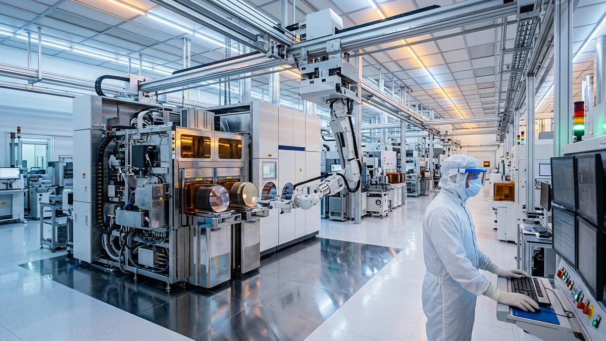
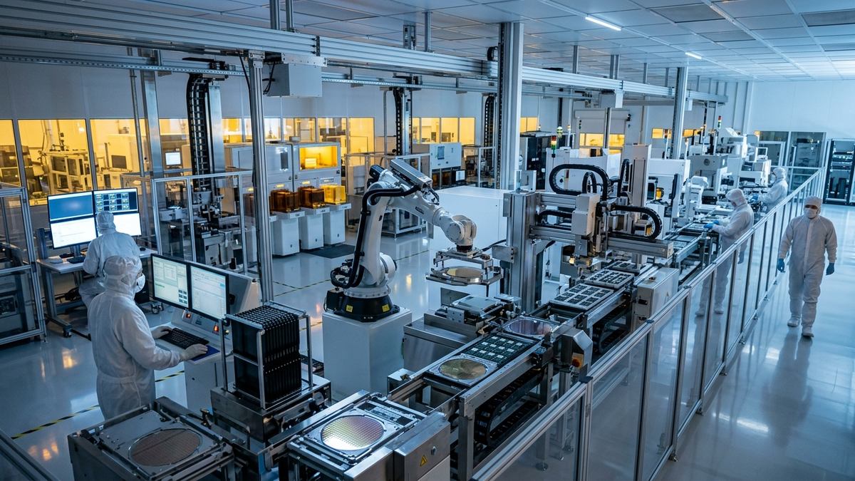
Spanning over 1,200 acres of prime industrial land, the park has been planned specifically to accommodate the extreme technical requirements of semiconductor cleanrooms and advanced electronics:
- Ultra-Pure Water and ZLD: Advanced wafer fabs consume millions of liters of ultra-pure water (UPW) daily. The corridor includes dedicated pipelines connected to the Ganga water network, integrated with Zero Liquid Discharge (ZLD) recycling facilities to ensure zero wastewater release into the environment.
- Multimodal Logistics Speed: Immediate proximity to Jewar International Airport ensures rapid air-cargo turnaround for high-value silicon wafers and microprocessors, while direct spurs to the Western Dedicated Freight Corridor facilitate heavy machinery transport from maritime ports in Gujarat and Maharashtra.
- Vibration-Damped Geotechnical Engineering: The industrial plots are pre-surveyed and reinforced with deep piling foundations to prevent micro-vibrations from nearby highways, ensuring nanometer-scale photolithography tools operate without optical distortion.
These infrastructure investments also create fertile ground for advanced electronic system-level design, complementing initiatives like Swadeza's AI-native semiconductor engineering tools.
Uttar Pradesh Electronics & Semiconductor Corridor: Strategic Infrastructure Benchmarks
The structured matrix below outlines the operational parameters, dedicated land allocations, and target manufacturing verticals across Uttar Pradesh's primary high-tech manufacturing nodes:
| Strategic Industrial Hub | Primary Manufacturing Verticals | Dedicated Land Footprint | Infrastructure Readiness | Competitive Advantage |
|---|---|---|---|---|
| YEIDA Sector 10 / 28 (Jewar) | OSAT/ATMP Facilities, Compound Semiconductor Fabs, Photonic Chips | 1,200+ Acres | Dedicated 400kV Substation, UPW Treatment, Multimodal Air Cargo | 10 mins from Jewar Airport; 75% land subsidy |
| Greater Noida Tech Zone | Enterprise AI Servers, High-Density PCB Fabrication, Power Modules | 450 Acres | Operational plug-and-play industrial park, optical fiber backbones | Mature engineering supply chain & talent pool |
| Noida Phase-II & SEZ | Surface Mount Technology (SMT), Mobile Handsets, Display Modules | 800+ Acres | Fully saturated industrial grid, automated logistics hubs | Produces >60% of domestic smartphone output |
| Lucknow-Kanpur Defense Corridor | Tactical Military Electronics, Rad-Hard Chips, Drone Avionics | 600 Acres | Defense industrial corridor clearances, testing ranges | Direct integration with DRDO and HAL facilities |
Bridging the Design-to-Manufacturing Pipeline
While peninsular technology capitals like Bengaluru and Hyderabad continue to dominate fabless semiconductor design, Uttar Pradesh is deliberately positioning itself as the mass manufacturing engine that turns design files into tangible silicon hardware.
The state is establishing specialized skill centers in collaboration with IIT Kanpur, IIT BHU, and leading polytechnic universities to train thousands of cleanroom technicians, vacuum maintenance engineers, and quality assurance inspectors.
As enterprises increasingly deploy on-premise hardware, the demand for embedded integration specialists—such as Forward-Deployed Engineers deploying complex technical systems—will surge across northern manufacturing corridors.
Through its aggressive blend of fiscal capital, world-class aviation logistics, and targeted infrastructure development, Uttar Pradesh is not merely participating in India's semiconductor journey; it is setting the operational pace for how states build high-tech industrial empires in the 21st century.
Frequently Asked Questions
What is Uttar Pradesh's policy framework for semiconductors and AI electronics?
Uttar Pradesh operates under its dedicated Semiconductor Policy (2024–2029) and Electronics Manufacturing Policy, which offer capital subsidies of up to 50% matching Central ISM approvals, 100% stamp duty exemptions, 75% land purchase rebates, and electricity duty waivers for 10 years.
Where are the key semiconductor and electronics hubs located in Uttar Pradesh?
The primary hub is centered around the Yamuna Expressway Industrial Development Authority (YEIDA) corridor in Sector 10 and Sector 28 near the upcoming Noida International Airport (Jewar), alongside established electronics manufacturing clusters in Greater Noida and Noida.
How does Uttar Pradesh plan to compete with southern and western states like Gujarat and Karnataka?
UP leverages its commanding 60% share of India's mobile phone production, an abundance of plug-and-play industrial land, rapid multimodal connectivity via Jewar Airport and the Western Dedicated Freight Corridor, and aggressive fiscal subsidies that eliminate upfront capital friction for global fab consortiums.
What specialized infrastructure is UP providing for chip foundries and cleanrooms?
The state is constructing dedicated dual 400kV and 220kV power substations guaranteeing uninterrupted power, zero-liquid discharge (ZLD) recycled water treatment plants supplying millions of liters of ultra-pure water daily, and specialized hazmat handling zones for semiconductor gases.
Primary Sources & Official References
- Uttar Pradesh Department of IT & Electronics: Semiconductor Policy 2024–2029 Implementation Directives and Financial Guidelines.
- India Semiconductor Mission (ISM): Comprehensive National Fab and ATMP Pipeline Assessment.
- Yamuna Expressway Industrial Development Authority (YEIDA): Master Plan 2041 & High-Tech Sector Land Allocation Registry.
- India Cellular & Electronics Association (ICEA): Electronics Hardware Manufacturing & Value-Add Analysis Report.