Teradyne Expands Semiconductor Presence in India: Global Automated Test Leader Opens Advanced Bengaluru Facility
By Sanjay Patel | Published September 15, 2026 | 8 min read
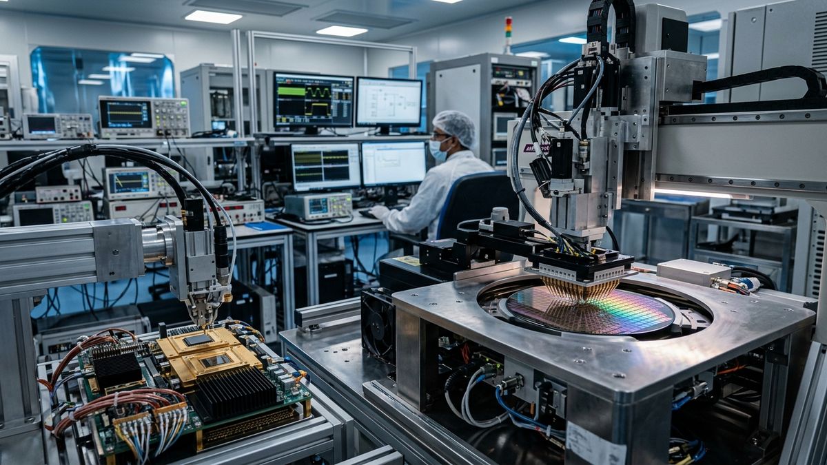
US semiconductor equipment leader Teradyne opens an advanced engineering and test facility in Bengaluru, expanding automated test systems, robotics automation, and post-silicon validation for India's chip ecosystem.
Teradyne (NASDAQ: TER), a global titan in semiconductor Automated Test Equipment (ATE) and advanced industrial robotics, has officially inaugurated a state-of-the-art engineering and operational facility in Bengaluru, significantly expanding its footprint to support India’s rapidly growing semiconductor manufacturing and packaging ecosystem. The new Bengaluru center serves as a premier engineering hub focused on developing next-generation automated test software, post-silicon validation architectures, robotic material handling, and custom test program development for global chipmakers and domestic foundry players.
The expansion arrives at a critical juncture for India's semiconductor ambitions. As multi-billion-dollar fabrication plants and Outsourced Semiconductor Assembly and Test (OSAT / ATMP) facilities break ground under the India Semiconductor Mission (ISM), Teradyne’s expanded presence provides the indispensable automated test infrastructure required to verify complex logic, radio-frequency (RF), automotive power, and memory integrated circuits before commercial release.
Automated Test Equipment (ATE): The Unsung Backbone of Chip Manufacturing
While front-end lithography and wafer fabrication often dominate public discourse, automated test equipment represents the ultimate arbiter of semiconductor commercial viability and yield economics. In modern microelectronics—where leading-edge microchips house billions of nanometer-scale transistors—fabrication imperfections are an unavoidable physical reality. Without rigorous, high-speed automated electrical testing, defective silicon dies escape to end products, risking catastrophic failures in automotive braking controllers, aerospace navigation units, medical hardware, and enterprise AI supercomputing clusters.
ATE systems operate during two critical phases of the semiconductor production lifecycle:
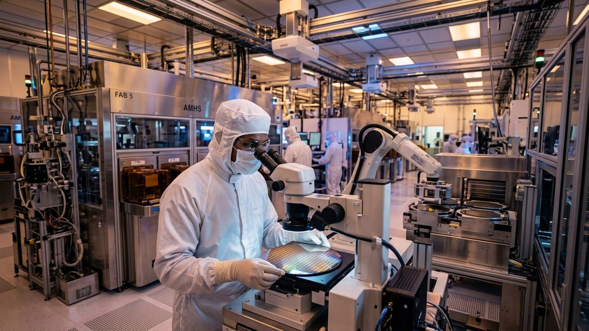
1. Wafer Probe / Sort (Front-End Testing): Before a raw silicon wafer is diced into individual dies, an ATE system uses ultra-fine microscopic probe cards to contact microscopic electrical test pads on every die, identifying functional circuits and mapping defects across the wafer.
2. Final Package Test (Back-End Testing): Once functional dies are packaged into protective casings with external ball grid arrays (BGAs) or pins, the ATE system subjects the completed chip to comprehensive thermal, electrical, and functional stress testing at high speeds.
"A semiconductor fab cannot function without world-class automated test engineering,"explained senior semiconductor industry analysts. "Every chip rolling off an assembly line must undergo exhaustive electrical interrogation in milliseconds. Teradyne's expansion in Bengaluru ensures that Indian engineering talent is directly designing the automated test software and hardware interfaces that validate the world's most advanced microprocessors."
Strategic Engineering Capabilities of Teradyne's New Bengaluru Facility
Teradyne’s newly expanded Bengaluru facility builds upon more than a decade of operational heritage in Karnataka, scaling technical headcount and lab infrastructure across several mission-critical semiconductor domains:
* Flagship ATE Platform Development: Engineering teams in Bengaluru contribute directly to the core software and hardware architecture of Teradyne’s industry-standard test platforms, including the UltraFLEX series (powering high-complexity smartphone application processors, AI neural accelerators, and 5G transceiver testing) and the J750 platform (the global benchmark for high-volume microcontroller testing).
* Post-Silicon Validation & Diagnostics: The facility provides advanced simulation and debugging environments for post-silicon test pattern generation, failure analysis, and timing verification, bridging the gap between electronic design automation (EDA) simulations and physical silicon behavior.
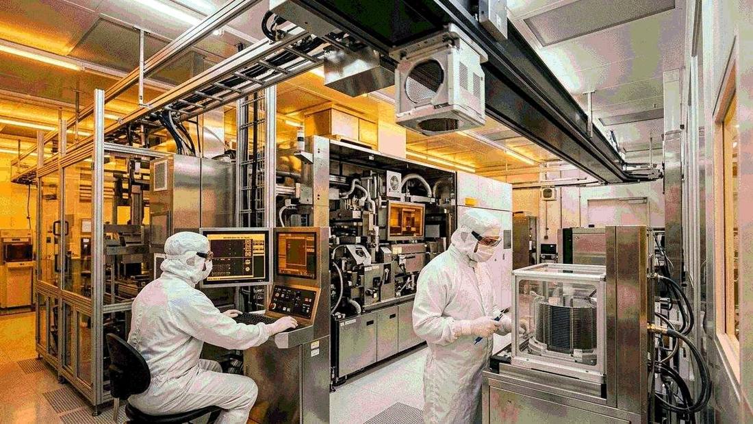
* Convergence of Robotics and Automated Material Handling: As the parent company of industrial robotics innovators Universal Robots (UR) and Mobile Industrial Robots (MiR), Teradyne’s Bengaluru center is integrating collaborative robotic arms and autonomous mobile robots (AMRs) into cleanroom test floors, automating the delicate transfer of silicon wafer cassettes and test socket changeovers with sub-millimeter precision.
* High-Density Power & Automotive IC Testing: With electric vehicles and renewable energy grids demanding robust silicon carbide (SiC) and gallium nitride (GaN) power semiconductors, the center is developing specialized high-voltage test modules capable of verifying power switching devices under extreme thermal stresses.
This deep integration of high-performance compute and hardware engineering parallels the structural shifts explored in our deep-dive analysis on quantum and AI infrastructure gaining momentum across Indian deeptech.
Operational Matrix: Semiconductor Testing & Infrastructure Enablers in India
The structured comparative matrix below outlines the operational requirements across chip manufacturing stages, Teradyne's technical architectures, and their strategic impact on India's electronics ecosystem:
| Semiconductor Phase | Core Equipment & Mechanism | Teradyne Platform Architecture | Indian Ecosystem Impact | Bengaluru Engineering Role |
|---|---|---|---|---|
| Wafer Sort / Die Probe | Multi-channel microscopic probe card interface | UltraFLEXplus / UltraFLEX Series | Maximizes yield for upcoming domestic fabs (Tata Dholera) | Custom high-speed digital pattern generation and timing calibration |
| Final Package Test | Automated thermal chamber & high-speed test sockets | J750 / Eagle Test Systems (ETS) | Enables high-throughput testing for ATMP/OSAT lines (Micron, CG Power) | Test program development, multi-site parallel testing optimization |
| Automotive & Power IC Test | High-voltage / high-current precision power modules | ETS-88 / ETS-364 Power Platforms | Supports domestic EV powertrain and energy grid power semiconductor validation | High-voltage transient stress testing and thermal runaway analysis |
| Cleanroom Automation | Autonomous Mobile Robots & Multi-axis Cobots | Universal Robots (UR) + MiR Robotics | Reduces human contamination and cycle time in Class 1/Class 10 cleanrooms | Robotics automation software and cleanroom robotic integration |
| Post-Silicon Failure Analysis | Time-domain reflectometry and automated fault isolation | Advanced Diagnostic Software Suite | Accelerates tape-out to commercial deployment cycle for domestic fabless startups | Defect classification algorithms and automated boundary-scan testing |
Catalyzing the India Semiconductor Mission: From Design to High-Volume Manufacturing
For over two decades, India has served as the back-office design powerhouse for the global semiconductor industry, housing over 20% of the world’s VLSI design talent across multinational design centers in Bengaluru, Hyderabad, and Noida. However, domestic engineers were historically isolated from physical manufacturing, assembly, and testing.
Teradyne’s deepened operational commitment bridges this historic divide. As projects under the India Semiconductor Mission come online—including the Tata Electronics joint venture fab in Dholera, the Micron ATMP facility in Sanand, the CG Power-Renesas OSAT facility in Sanand, and Kaynes Semicon's unit in Sanand—the demand for local ATE test engineering, socket design, and probe interface hardware has surged.
Furthermore, Teradyne’s testing platforms are actively utilized across cutting-edge domestic R&D facilities, including the recently inaugurated HCLTech Advanced Semiconductor Lab in Bengaluru, which leverages Teradyne equipment to deliver comprehensive post-silicon engineering, electrical characterization, and failure analysis to global fabless clients.
The regional clustering of these advanced facilities reinforces Bengaluru’s status as the nerve center of Indian technology, while complementing the national momentum highlighted in our study of how hardware ventures are expanding beyond traditional hubs across emerging industrial corridors.
Strategic Outlook: Securing India's Position in the Global Semiconductor Supply Chain
As geopolitical realignments push global technology enterprises toward "China+1" supply chain diversification, testing and packaging infrastructure has emerged as the fastest pathway to establishing semiconductor manufacturing credibility. Automated test systems represent high-margin, sticky capital investments that anchor manufacturing ecosystems for decades.
With its expanded Bengaluru office, Teradyne is not merely augmenting its customer support capacity; it is positioning India as a strategic global development hub for automated test software and robotics automation.
By coupling India's world-class software engineering capabilities with advanced physical test instrumentation, initiatives like Teradyne's expansion ensure that India will not only design the microchips of tomorrow, but verify, validate, and package them for global markets.