India’s GaN Chip Push Gathers Momentum as Spintronics AI and CSIR-CEERI Target Indigenous Fabrication
By Sanjay Patel | Published October 3, 2026 | 8 min read
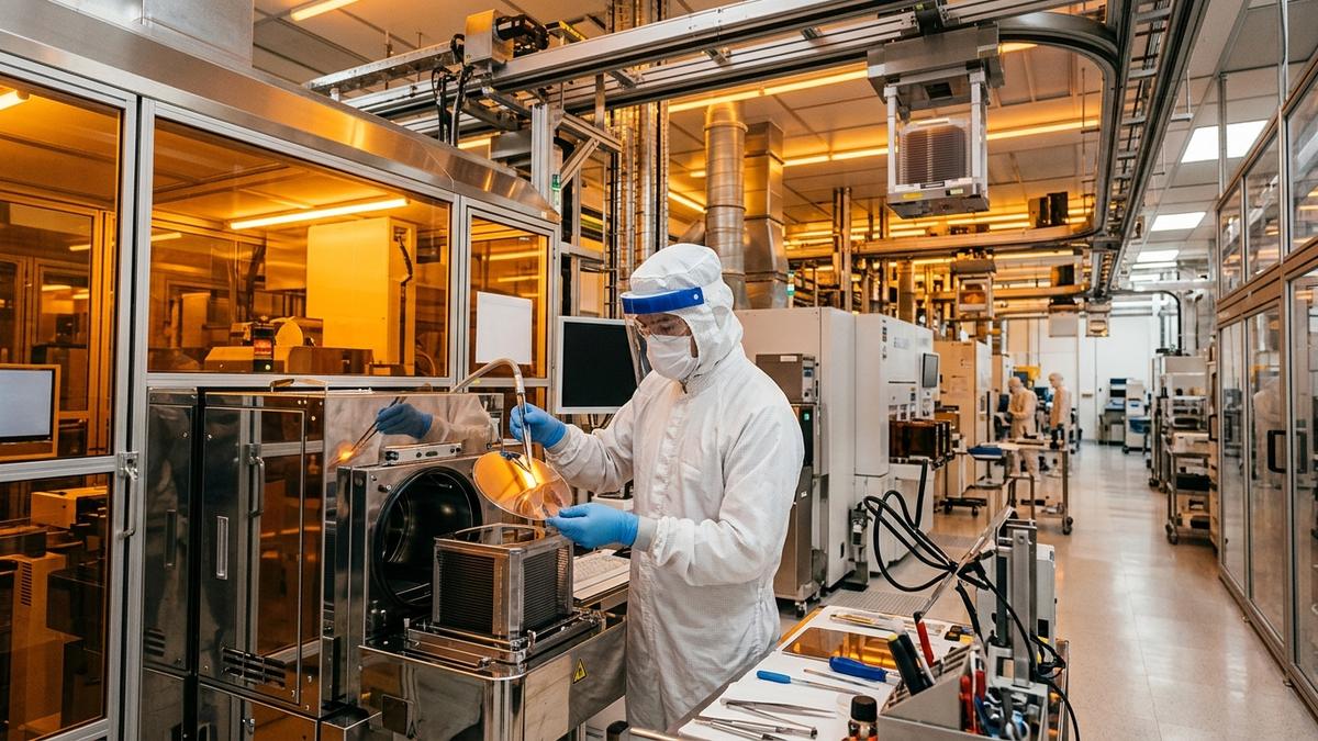
Spintronics AI and CSIR-CEERI forge a landmark alliance to transition laboratory gallium-nitride research into an indigenous commercial semiconductor fabrication facility.
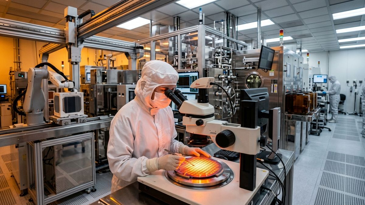
India's strategic campaign to establish indigenous capabilities across wide-bandgap (WBG) compound semiconductors has gained substantial momentum, driven by a landmark collaboration between Hyderabad-based deeptech startup Spintronics AI Semiconductors and the CSIR-Central Electronics Engineering Research Institute (CSIR-CEERI), Pilani. Under the formalized agreement, the organizations will establish a commercial technology and design transfer framework to translate over two decades of institutional GaN research into mass-market electronics, while conducting comprehensive feasibility evaluations for building India's first dedicated indigenous GaN fabrication foundry.
The partnership arrives as global electronics supply chains undergo a structural transition away from legacy silicon towards wide-bandgap materials like Gallium Nitride (GaN) and Silicon Carbide (SiC). With the Indian domestic GaN market projected to surge from roughly $224 million in 2026 to nearly $1.88 billion by 2033, securing sovereign fabrication capabilities has emerged as a top national industrial priority.
Breaking Silicon's Physical Ceiling
For more than half a century, silicon (Si) has served as the undisputed workhorse of the global semiconductor industry. However, in high-power, high-voltage, and high-frequency environments, silicon is colliding with immutable physical limitations. As power densities surge in electric vehicle powertrains, hyperscale data centre power delivery units (PDUs), and 5G/6G wireless communication arrays, silicon transistors suffer from prohibitive thermal dissipation losses and low breakdown thresholds.
Gallium Nitride overcomes these bottlenecks through fundamentally superior material physics:
- Wide Bandgap Energy (3.4 eV): GaN features an electronic bandgap three times wider than silicon (1.1 eV), allowing devices to withstand electric breakdown fields nearly an order of magnitude stronger without catastrophic breakdown.
- Superior Electron Velocity & Mobility: Higher electron mobility allows GaN transistors to switch at frequencies exceeding several megahertz, dramatically shrinking the size of surrounding inductive coils and capacitors.
- Unrivaled Thermal and Energy Efficiency: In power conversion circuits, GaN reduces power switching losses by 40% to 60%, eliminating bulky cooling systems and delivering ultra-compact form factors.
This technological frontier aligns directly with national policy goals, where India's semiconductor push creates extensive supply chain opportunities across materials and specialized foundries and strengthens domestic initiatives that target over 200 fabless chip design startups under ISM 2.0.
"Gallium Nitride is the defining semiconductor substrate of the clean energy and electrified mobility revolution,"stated senior scientists at CSIR-CEERI. "By bridging our institutional cleanroom IP with Spintronics AI's commercial product engineering, we are ensuring India transforms from a technology importer into an exporter of high-power semiconductor intellectual property."
Technical & Commercial Parameters: GaN vs Silicon vs Silicon Carbide
The operational and financial comparison below illustrates why GaN represents the highest return on domestic capital investment:
| Material Parameter | Silicon (Si) Standard | Gallium Nitride (GaN) | Silicon Carbide (SiC) | Strategic Commercial Impact |
|---|---|---|---|---|
| Energy Bandgap (eV) | 1.12 eV | 3.40 eV | 3.26 eV | GaN withstands extreme operating voltages |
| Breakdown Electric Field | 0.3 MV/cm | 3.3 MV/cm | 3.0 MV/cm | 10x higher dielectric breakdown resistance |
| Electron Mobility | 1,400 cm²/V·s | 2,000 cm²/V·s | 900 cm²/V·s | Ultra-fast switching in RF and power converters |
| Thermal Dissipation | Baseline Reference | High Efficiency | Exceptional | Replaces liquid cooling with passive heatsinks |
| Typical Target Vertical | Logic & Consumer Microcontrollers | Fast Charging, EV Inverters, 5G RF | High-Voltage Locomotives & Heavy Grid | GaN addresses broad commercial sweet spot |
| Fab Facility Capital Capex | $3B – $12B+ | $150M – $350M | $500M – $1.5B | Compound fabs are highly cost-effective |
Blueprint for an Indigenous Open-Access GaN Fab
A decisive focus of the Spintronics AI and CSIR-CEERI initiative is evaluating techno-commercial blueprints for an open-access indigenous GaN fabrication foundry located in India:
- Epitaxial Optimization on Silicon Substrates (GaN-on-Si): Leveraging 150mm (6-inch) and 200mm (8-inch) silicon wafers to grow defect-free GaN crystalline layers via Metal-Organic Chemical Vapor Deposition (MOCVD), drastically reducing production costs compared to native GaN substrates.
- Pilot Prototyping Line: Utilizing CSIR-CEERI's cleanroom infrastructure in Pilani to execute device packaging, parameter extraction, and reliability qualifications adhering to automotive AEC-Q101 standards.
- Open-Access Shared Foundry Model: Establishing a domestic foundry infrastructure where Indian fabless chip startups, defense research laboratories (DRDO), and space agencies can tape out power switches and monolithic microwave integrated circuits (MMICs) without sending sensitive design files to foreign foundries.
The capital expenditure dynamics of compound semiconductors strongly favor domestic deployment. While digital silicon megafabs—such as those spearheaded by Tata Electronics in Dholera—require over $10 billion in capital and high-volume digital consumption, a specialized GaN compound fab can achieve commercial viability with an investment of under $350 million.
Critical Impact on Defense, Automotive, and 6G Communications
The downstream ramifications of domestic GaN chip production span India's most critical industrial and strategic sectors. In electric mobility, GaN on-board chargers can reduce vehicle charging times by 50% while shedding kilograms of thermal management weight, extending overall battery range for domestic two-wheeler and four-wheeler fleets.
In aerospace and defense, GaN-based active electronically scanned array (AESA) radars deliver vastly superior target detection range, resolution, and jam resistance compared to legacy traveling-wave tubes. Similarly, in telecommunications, deploying GaN power amplifiers across 5G and future 6G base stations cuts operational power consumption by thousands of megawatts across pan-India cellular networks.
By combining institutional scientific depth with entrepreneurial execution, Spintronics AI and CSIR-CEERI are positioning India at the vanguard of the global compound semiconductor revolution.
Frequently Asked Questions
What is the strategic objective of the Spintronics AI and CSIR-CEERI partnership?
The alliance aims to establish a commercial technology transfer framework that transitions CSIR-CEERI's advanced laboratory research in Gallium Nitride (GaN) into production-ready semiconductor devices, while evaluating the feasibility of setting up an open-access indigenous GaN fabrication foundry in India.
Why is Gallium Nitride (GaN) critical for next-generation electronics?
GaN is a wide-bandgap compound semiconductor that can handle significantly higher voltages, operating temperatures, and switching frequencies than traditional silicon, while reducing electrical power losses by up to 50% and shrinking thermal component footprints.
What is the projected size of the Indian GaN semiconductor market?
Market projections estimate that India's domestic GaN market will expand from approximately $224 million in 2026 to nearly $1.88 billion by 2033, driven by rapid adoption in electric vehicle power electronics, telecommunications infrastructure, renewable energy, and defense.
How does GaN fabrication differ financially from silicon foundries?
While leading-edge digital silicon foundries require tens of billions of dollars in capital expenditure, compound semiconductor fabs for GaN can be established for $150 million to $350 million, making domestic fabrication achievable on faster capital cycles.
Primary Sources & Official References
- CSIR-Central Electronics Engineering Research Institute (CSIR-CEERI): Wide-Bandgap Semiconductor Division and Microelectronics Laboratory.
- Spintronics AI Semiconductors: Commercial Gallium Nitride Strategic Roadmap and Design Filing.
- India Semiconductor Mission (ISM): Compound Semiconductor & Silicon Carbide / GaN Advisory Framework.
- Ministry of Electronics and Information Technology (MeitY): National Microelectronics and Advanced Hardware Policy.