Spintronics AI Partners With CSIR-CEERI to Commercialize Production-Ready GaN Chips and Explore Indigenous Fab
By Karthik Ramaswamy | Published October 2, 2026 | 8 min read
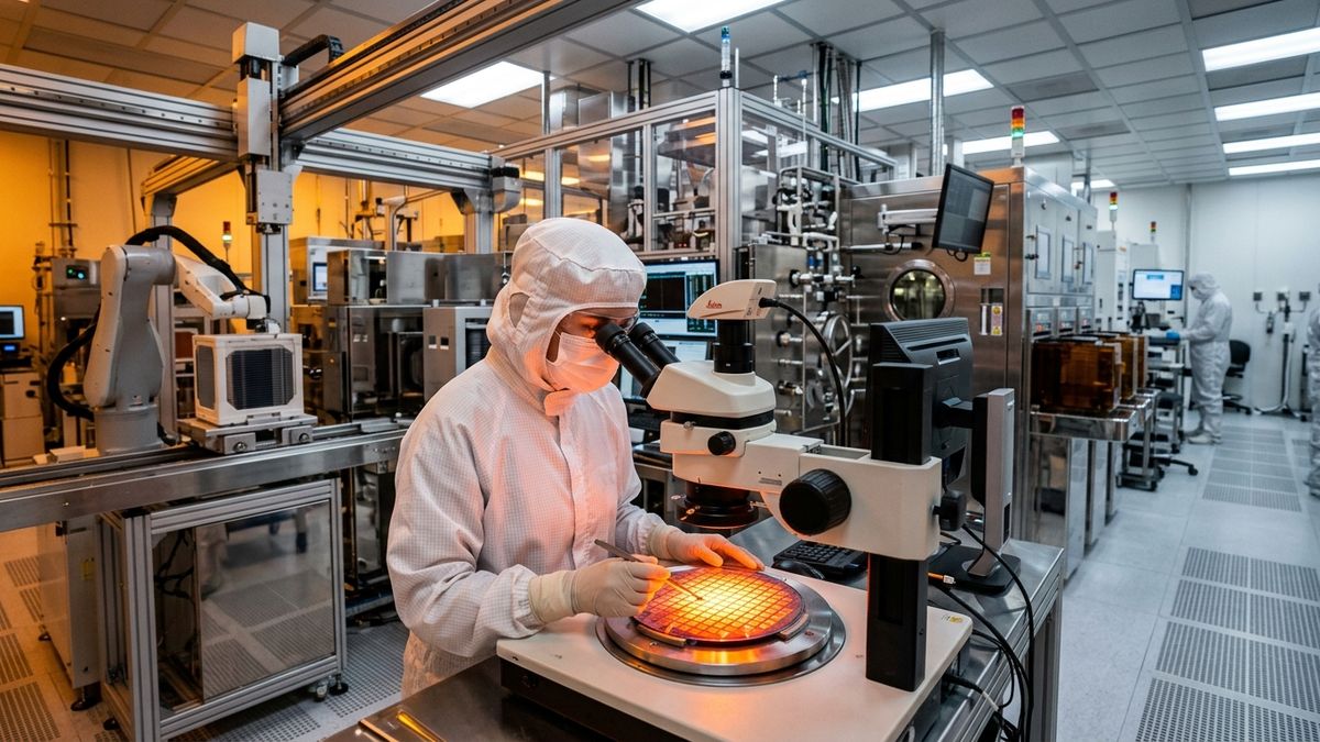
Hyderabad-based Spintronics AI and CSIR-CEERI join forces to advance production-ready gallium nitride semiconductor technology and explore establishing an indigenous GaN fabrication foundry.
Hyderabad-based deeptech venture Spintronics AI has formalized a strategic partnership with the CSIR-Central Electronics Engineering Research Institute (CSIR-CEERI), Pilani, to accelerate the commercialization of production-ready Gallium Nitride (GaN) semiconductor devices and explore setting up an indigenous GaN fabrication foundry. The agreement unites Spintronics AI's proprietary power architecture designs with CSIR-CEERI's decades of compound semiconductor research, targeting mission-critical applications in electric mobility, green energy conversion, and next-generation telecommunications.
As the global electronics industry aggressively transitions toward wide-bandgap (WBG) semiconductors, Gallium Nitride has emerged as the premier material capable of replacing legacy silicon in power management and high-frequency RF transmission. By developing indigenous GaN epitaxy and device packaging capabilities domestically, the alliance aims to plug a critical hardware vulnerability in India's semiconductor value chain.
Breaking Silicon Limits: The Physics and Economics of GaN
Traditional silicon power transistors are reaching their fundamental thermodynamic limits. In high-voltage environments, silicon MOSFETs suffer from substantial switching losses, large parasitic capacitances, and significant heat generation, necessitating heavy cooling systems and oversized inductive components.
Gallium Nitride completely fundamentally shifts these physical parameters:
- Wide Energy Bandgap: GaN features a 3.4 eV bandgap—triple that of silicon (1.1 eV)—enabling the material to withstand electric breakdown fields nearly ten times higher.
- High Electron Mobility: Electrons navigate through GaN crystals at vastly higher velocities, permitting switching frequencies exceeding 1 MHz without runaway thermal penalties.
- Dramatic Miniaturization: In EV traction inverters and consumer chargers, GaN power stages reduce magnetic component volume by 40% to 60%, delivering lighter, more efficient power assemblies.
This technical breakthrough dovetails with the national semiconductor push, where India targets 200 chip-design companies under ISM 2.0 and creates new domestic supply chain opportunities across materials and fabs. While digital CMOS logic demands billion-dollar multi-node megafabs, compound semiconductor fabs for GaN can be established at a fraction of the cost, making commercial manufacturing viable within rapid timelines.
Material & Performance Matrix: Silicon vs Gallium Nitride (GaN) vs Silicon Carbide (SiC)
The table below illustrates why compound semiconductors are rapidly displacing silicon across power and RF applications:
| Semiconductor Characteristic | Silicon (Si) Standard | Gallium Nitride (GaN) | Silicon Carbide (SiC) | Operational Advantage of GaN |
|---|---|---|---|---|
| Energy Bandgap (eV) | 1.12 | 3.40 | 3.26 | 3x Higher Dielectric Strength |
| Critical Breakdown Field (MV/cm) | 0.3 | 3.3 | 3.0 | 10x Higher Voltage Tolerance |
| Electron Mobility (cm²/V·s) | 1,400 | 2,000 | 900 | Ultra-Fast Switching Frequencies |
| Thermal Dissipation Efficiency | Moderate | High | Ultra-High | Eliminates Bulky Heatsinks |
| Typical Target Frequency | < 100 kHz | 500 kHz – 10 GHz | < 500 kHz | Ideal for 5G/6G & EV Power |
| Capex per Fab Facility | $3B – $10B+ | $150M – $350M | $500M – $1.5B | High Return on Domestic Capital |
"Commercializing Gallium Nitride is not merely an engineering milestone; it is an economic and sovereign imperative,"stated technical directors at CSIR-CEERI. "By combining CEERI's cleanroom fabrication heritage with Spintronics AI's commercial market execution, we are creating a direct bridge from laboratory wafer prototypes to industrial scale."
Blueprint for an Indigenous Open-Access GaN Foundry
A central pillar of the Spintronics AI and CSIR-CEERI roadmap is evaluating the commercial viability of an indigenous GaN foundry facility:
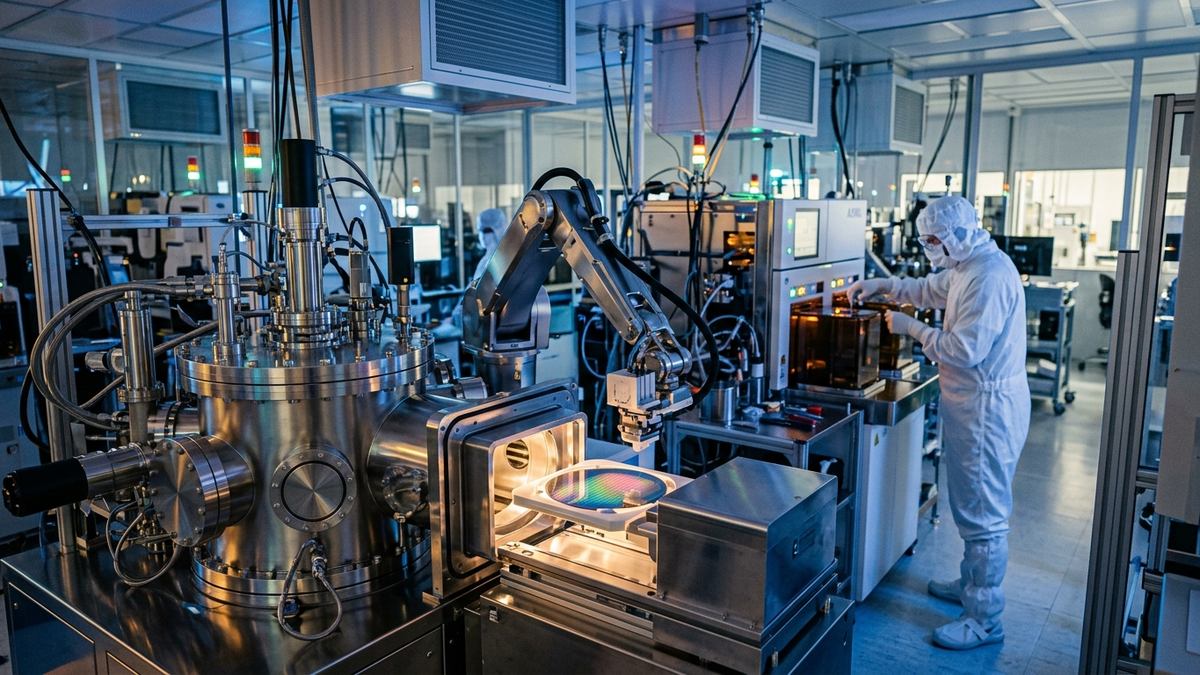
- Epitaxial Growth on Silicon (GaN-on-Si): Utilizing standard 150mm (6-inch) and 200mm (8-inch) silicon substrate wafers, the team is optimizing metal-organic chemical vapor deposition (MOCVD) growth recipes to minimize lattice mismatch and wafer bow.
- Pilot Prototyping Line: Establishing a pilot fabrication line at CEERI's Rajasthan cleanrooms to qualify device reliability according to AEC-Q101 automotive standards.
- Commercial Spin-Out Model: Structuring an open-access foundry model where domestic fabless chip startups can tape out power switches and RF monolithic microwave integrated circuits (MMICs) without sending IP to overseas fabs.
This compound semiconductor momentum complements major commercial industrial investments, such as Tata Electronics building India's semiconductor ecosystem and edge semiconductor design centres like Mythic AI's analog compute expansion in Bengaluru.
Strategic Value for India's Automotive and Telecom Infrastructure
The practical implications of domestically fabricated GaN chips are immense. In India's fast-growing two-wheeler and four-wheeler electric mobility sectors, battery range and charging speed are governing consumer purchase metrics. GaN-based on-board chargers can recharge vehicle batteries in half the time while shedding kilograms of payload weight.
Simultaneously, in telecommunications, 5G and future 6G cell towers require massive MIMO antenna arrays that consume vast amounts of electrical power. GaN RF power amplifiers operate with significantly higher power-added efficiency (PAE), lowering operating expenditures for telecom carriers across pan-India deployments. By proving out production-ready GaN devices, Spintronics AI and CSIR-CEERI are anchoring India's transition from a chip consumer to an advanced compound semiconductor creator.
Frequently Asked Questions
What is Gallium Nitride (GaN) and why is it superior to conventional silicon?
Gallium Nitride (GaN) is a wide-bandgap compound semiconductor with an energy bandgap of 3.4 electron-volts, compared to 1.1 eV for silicon. This allows GaN devices to operate at significantly higher voltages, temperatures, and switching frequencies while drastically reducing power conversion losses and heat dissipation.
What are the primary applications of GaN chips developed by Spintronics AI and CSIR-CEERI?
Primary applications include electric vehicle (EV) traction inverters, fast on-board chargers, solar power inverters, high-efficiency data centre power delivery units (PDUs), and 5G/6G radio-frequency (RF) power amplifiers.
What role does CSIR-CEERI play in this partnership?
CSIR-CEERI (Pilani) provides institutional cleanroom facilities, advanced materials characterization equipment, electron microscopy, and decades of semiconductor process engineering IP to refine GaN epitaxial recipes and device prototyping.
How does an indigenous GaN fab fit into the India Semiconductor Mission (ISM)?
While major silicon fabs like Tata Electronics focus on large-scale digital silicon at 28nm nodes, GaN compound semiconductor fabs require substantially lower capital expenditure (under $300M) while addressing high-value, strategic automotive, industrial, and defense markets.
Primary Sources & Official References
- CSIR-Central Electronics Engineering Research Institute (CSIR-CEERI): Wide-Bandgap Semiconductor Division.
- Spintronics AI: Commercial Gallium Nitride Strategic Roadmap & Tape-Out Filing.
- India Semiconductor Mission (ISM): Compound Semiconductor and Silicon Carbide / GaN Focus Group.
- IEEE Electron Devices Society: High-Voltage GaN-on-Silicon Power Device Characterization.