IIT Bombay unveils a dedicated semiconductor deep-tech accelerator backed by SINE, providing fabless chip startups with multi-project wafer shuttles, EDA tool access, and cleanroom testbeds.
Executive Key Takeaways
- IIT Bombay's SINE will incubate 25 fabless semiconductor and RISC-V silicon startups annually with prototyping grants up to ₹1.5 crore per team.
- Participating ventures receive subsidized access to advanced electronic design automation (EDA) tools through the national ChipIN EDA center.
- The program provides guaranteed multi-project wafer (MPW) shuttle runs with global commercial foundries to de-risk physical silicon tape-out.
IIT Bombay Launches Semiconductor-Focused Deep-Tech Accelerator to Advance Sovereign Silicon and Fabless Startups marks a critical structural milestone in India's quest to build a self-reliant microelectronics design ecosystem. Hosted by the premier institute's Society for Innovation and Entrepreneurship (SINE) in Mumbai, the newly inaugurated accelerator program represents a dedicated institutional vehicle designed to bridge the capital-intensive chasm between academic chip design and commercial silicon production.
While commercial fabrication initiatives like India's approved semiconductor projects across six states and the expansion of domestic EDA tools under ChipIN establish physical foundry infrastructure, design IP remains the primary driver of value in modern electronics. IIT Bombay's program addresses the prohibitive upfront costs of electronic design automation (EDA) tooling and prototype tape-outs, enabling 25 promising Indian fabless ventures to build market-ready silicon every year.
Overcoming the CapEx Barrier in Chip Prototyping
Developing a custom application-specific integrated circuit (ASIC) or system-on-chip (SoC) typically requires millions of dollars in software licensing fees and mask tooling costs before a single functional prototype is manufactured. For early-stage Indian ventures, this capital barrier has historically forced engineering talent into software services rather than deep hardware innovation.
The SINE accelerator dismantles these bottlenecks through a multi-tiered infrastructure model:
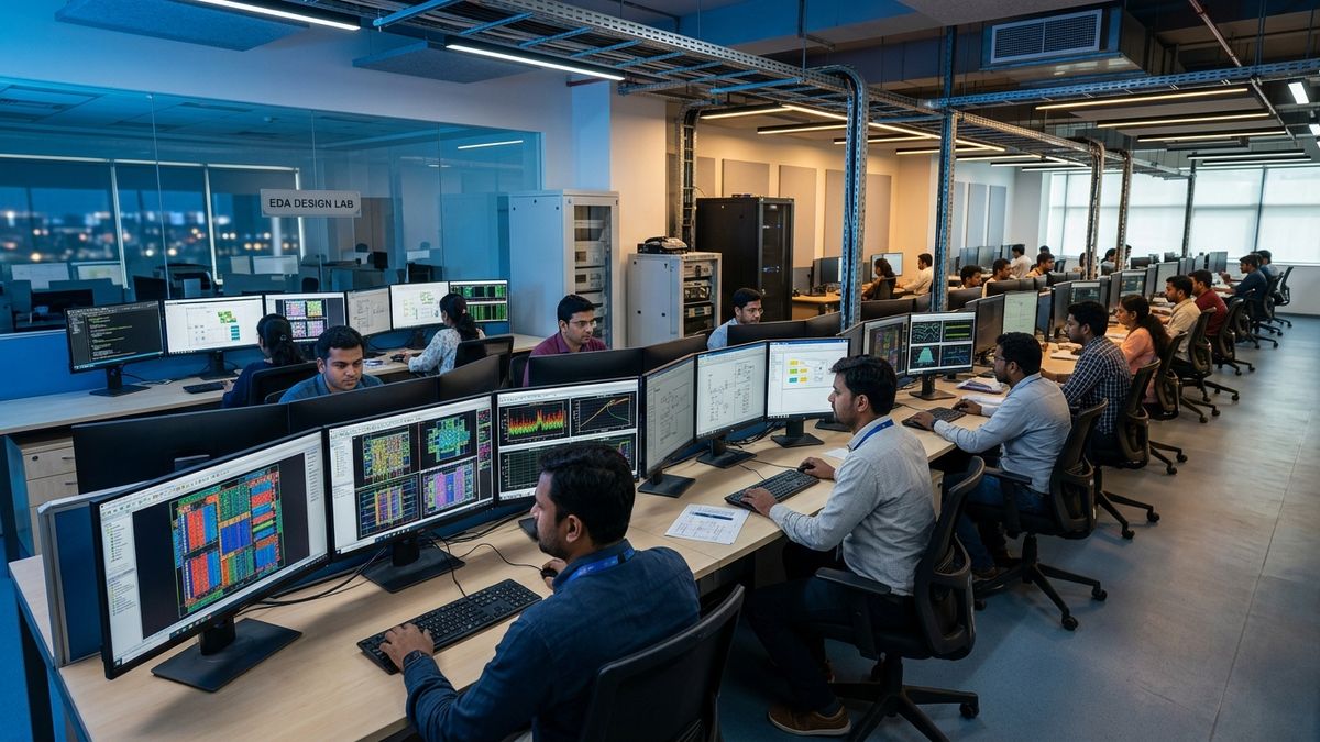
- Subsidized EDA Tool Access: Through partnerships with the national ChipIN EDA center, startups access industry-standard verification and layout tool suites (Cadence, Synopsys, Siemens) at nominal operational costs.
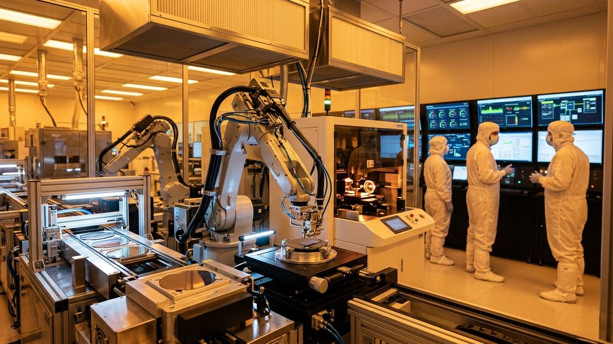
- Multi-Project Wafer (MPW) Shuttle Integration: By aggregating multiple startup designs onto shared silicon wafers, the accelerator reduces physical tape-out expenditures by up to 85%, allowing rapid iterative hardware validation.
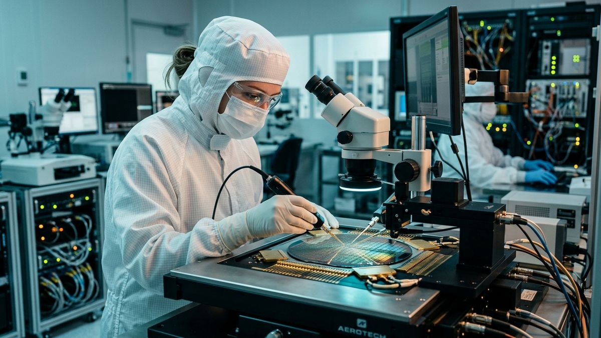
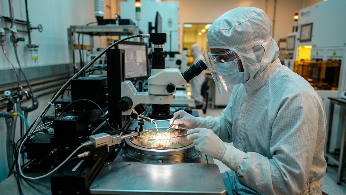
- Post-Silicon Characterization Cleanrooms: Startups leverage IIT Bombay's Centre for Excellence in Nanoelectronics (CEN) for high-frequency testing, thermal characterization, and failure analysis under cryogenic and industrial conditions.
"Silicon design is the intellectual bedrock of modern geopolitical power,"declared academic leaders at IIT Bombay. "Through this accelerator, we are ensuring that Indian engineers are not merely writing firmware for foreign architectures, but designing the sovereign RISC-V processors, power management chips, and telecom SoCs that power our nation's digital infrastructure."
Technical Architecture & Program Specifications
The accelerator targets four strategic technology verticals that directly support domestic industrial supply chains and national security priorities.
The structured overview below outlines the accelerator's architectural priorities and cohort parameters:
| Program Dimension | Cohort Specification | Strategic Infrastructure Component | Industrial Target Area |
|---|---|---|---|
| Cohort Velocity | 25 Startups Per Annum | SINE DeepTech Incubator & IIT Bombay CEN | Commercial Silicon Tape-Out |
| Prototyping Grants | Up to ₹1.5 Cr per Startup | Viability Gap & MeitY DLI Capital | Multi-Project Wafer Fabrications |
| Architecture Focus | Open-Standard RISC-V | Shakti & Vega Core Implementations | Sovereign Automotive & IoT Nodes |
| Process Nodes | 28nm, 65nm, and 180nm | Global & Domestic Foundry Shuttles | Industrial, Telecom & Consumer Chips |
| Testing Facilities | Class 100/1000 Cleanrooms | Automated Probe Stations & Spectrum Analyzers | Commercial Mil-Spec Compliance |
Synergies with India Semiconductor Mission 2.0
The launch of the IIT Bombay accelerator directly reinforces the national objectives of the India Semiconductor Mission (ISM 2.0). By providing a structured talent and design pipeline, the accelerator creates captive domestic demand for packaging facilities and commercial fabs currently under construction, mirroring achievements such as the unveiling of India's homegrown broadband chip Vihaan-I.
Startups incubated within the program will gain direct entry into government procurement frameworks under the Public Procurement (Preference to Make in India) order. This regulatory pathway provides domestic chip design firms with guaranteed commercial access to state telemetry deployments, smart electrical metering infrastructure, and naval communications contracts.
Long-Term Impact on National Hardware Sovereignty
As global supply chains navigate geopolitical decoupling and export restrictions, sovereign semiconductor capability has transitioned from a commercial priority into a strategic national imperative. IIT Bombay's accelerator institutionalizes a repeatable, de-risked methodology for semiconductor entrepreneurship in India.
By systematically reducing prototype iteration cycles from years to months, the initiative equips Indian founders to develop high-margin, internationally competitive hardware intellectual property. In doing so, it firmly anchors Mumbai and the western manufacturing corridor alongside Bengaluru as frontline hubs of Asian silicon engineering.
Frequently Asked Questions
What core resources does the IIT Bombay semiconductor accelerator provide?
Startups receive dedicated EDA software licenses (Synopsys, Cadence, Siemens EDA), subsidized participation in multi-project wafer (MPW) shuttles for physical chip tape-out, access to IIT Bombay's nano-fabrication cleanroom testbeds, and mentorship from veteran silicon architects.
How does the accelerator align with the India Semiconductor Mission (ISM)?
The program directly implements ISM's Design Linked Incentive (DLI) mandate, which seeks to nurture over 100 domestic fabless chip design ventures to ensure Indian IP powers commercial electronics, electric vehicles, telecom infrastructure, and defense systems.
What silicon architectures are prioritized in the initial cohort?
The accelerator is prioritizing RISC-V sovereign processor cores, power management integrated circuits (PMICs) for automotive EV platforms, neuromorphic AI inference silicon, and RF frontend modules for 5G/6G satellite communications.
Who is eligible to apply for the SINE semiconductor accelerator?
Eligibility is open to early-stage deeptech startups, academic spin-outs from Indian engineering universities, and experienced VLSI engineering teams incorporated in India with a clear semiconductor design IP roadmap.
Primary Sources & Official References
- IIT Bombay Society for Innovation and Entrepreneurship (SINE) Official Announcement: Accelerator launch disclosure and incubation charter (https://sineiitb.org).
- India Semiconductor Mission (ISM) Design Linked Incentive (DLI) Policy Framework: Official MeitY semiconductor design support guidelines (https://ism.gov.in).
- Ministry of Electronics and Information Technology (MeitY) ChipIN Centre Portal: National EDA infrastructure access program (https://www.meity.gov.in).