Raana Semiconductors Targets ₹100 Crore Series A: Homegrown Deeptech Startup in Talks to Scale 12-Inch Silicon Crystal-Growth Technology
By Sanjay Patel | Published August 22, 2026 | 8 min read
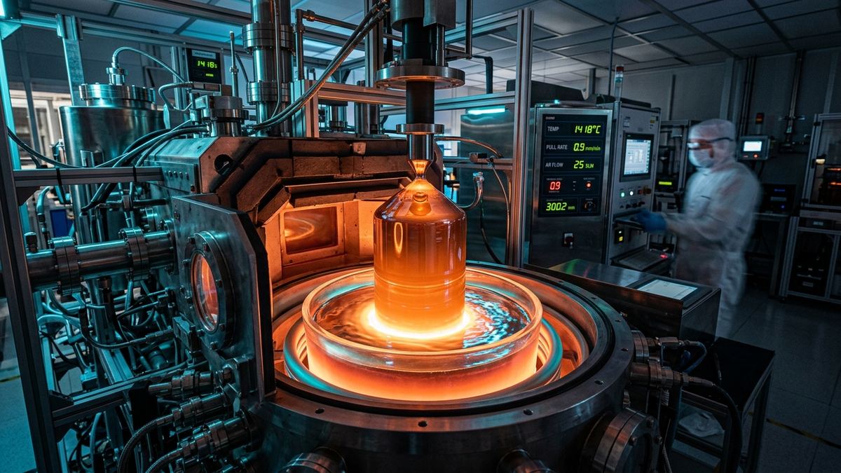
Raana Semiconductors advances talks for a ₹100 crore Series A round to scale India's first indigenous 12-inch (300mm) single-crystal silicon ingot growth furnaces for wafer fabrication.
BENGALURU — While India's semiconductor ambitions have gained massive momentum through multi-billion-dollar approvals for commercial fabrication plants and packaging units, one critical vulnerability has remained unaddressed: the absolute domestic absence of semiconductor-grade monocrystalline silicon ingots and raw 300mm (12-inch) wafer manufacturing.
Aiming to solve this foundational upstream bottleneck, Bengaluru and Noida-headquartered semiconductor materials and equipment startup Raana Semiconductors is reportedly in advanced discussions with leading domestic deeptech venture funds, industrial family offices, and strategic conglomerates to raise a ₹100 crore ($12 million) Series A funding round.
The fresh capital will be dedicated to scaling commercial production and customer qualification of Raana's proprietary 12-inch Czochralski (CZ) silicon crystal-growth furnaces and precision wafer slicing equipment—a critical technological breakthrough that could provide India with end-to-end sovereign control over raw semiconductor substrate manufacturing.
De-risking India's Semiconductor Substrate Blind Spot
Over the past three years, the India Semiconductor Mission (ISM) has sanctioned over a dozen high-profile fabrication and OSAT facilities, including Tata Electronics' mega-fab in Dholera, Micron's testing unit in Sanand, and CG Power's assembly facility, as documented in India's Semiconductor Push Accelerates with 12 Approved Projects.
However, virtually 100% of the raw monocrystalline silicon wafers required to feed these cleanrooms must currently be imported from a tight oligopoly of manufacturers in Japan (Shin-Etsu, SUMCO), Taiwan (GlobalWafers), Germany (Siltronic), and South Korea (SK Siltron). In times of geopolitical friction or shipping choke-points, wafer supply shocks can bring multi-billion-dollar fabs to a complete halt.
Raana Semiconductors was founded by veteran materials scientists and precision thermal engineers to develop homegrown high-purity crystal growth systems capable of producing Electronic-Grade Silicon (EG-Si) ingots with 99.9999999% (9N to 11N) purity.
"A semiconductor fab without a sovereign silicon wafer supply is like a state-of-the-art printing press without paper,"said a senior technical advisor at Raana Semiconductors. "Growing a 300mm single-crystal silicon boule is among the most demanding thermodynamic challenges in modern physics. By mastering the furnace mechanics, magnetic stabilization, and thermal gradients indigenously, we are securing the foundational bedrock of India's silicon sovereignty."
The Engineering Challenge: Mastering the Czochralski Ingot Puller
Growing a 12-inch electronic-grade silicon crystal ingot requires pulling a solid single crystal from a bath of molten polysilicon heated to over 1,425°C (2,597°F) inside a quartz crucible under a high-purity argon vacuum atmosphere.
Raana's proprietary furnace architecture incorporates several proprietary engineering innovations:
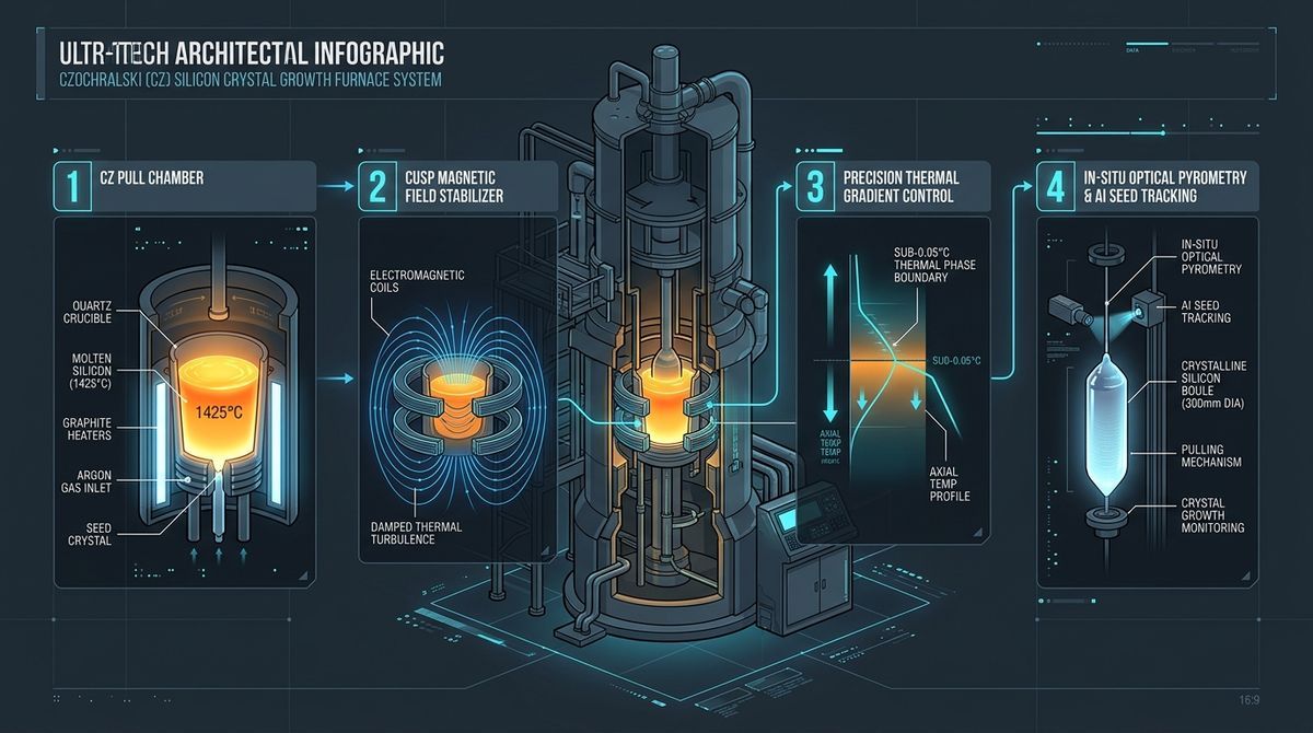
- Cusp Magnetic Field Stabilization: Applying high-strength electromagnetic fields to damp turbulent convective currents in the molten silicon bath, ensuring uniform radial dopant distribution.
- Ultra-Fine Thermal Gradient Control: Maintaining temperature tolerances within ±0.05°C across the liquid-solid phase boundary to prevent crystal lattice dislocations and point defects.
- Diamond Wire Multi-Wafer Slicing: Developing automated multi-wire slicing machines that saw monocrystalline ingots into 775-micrometer thin wafers with sub-micron surface roughness and negligible kerf loss.
Technical Specifications: Raana 12-Inch CZ Growth Benchmarks
The operational and metallurgical parameters achieved by Raana’s prototype growth reactors compared against Tier-1 global standards are detailed in the benchmark table below:
| Technical Parameter | Global Tier-1 Standard (Shin-Etsu / SUMCO) | Raana Semiconductors CZ Reactor | Commercial Significance |
|---|---|---|---|
| Ingot Diameter | 300 mm (12-inch) | 300 mm (12-inch) | Standard substrate size for sub-28nm fabs |
| Silicon Purity Level | 11N (99.999999999%) | 9N – 11N Electronic Grade | Minimizes electron scattering & gate leakage |
| Dislocation Density | Zero Dislocations (Dash Technique) | Zero Dislocation Structure Verified | Critical for high-yield photolithography |
| Oxygen Concentration (Oi) | 10 to 16 ppma (controlled) | 11.5 – 13.8 ppma | Prevents wafer warpage during high-temp anneals |
| Pull Rate Velocity | 0.8 – 1.2 mm/min | 0.95 mm/min (Automated) | High-throughput commercial ingot yield |
| Target Fab Integrations | TSMC, Intel, Samsung | Tata-PSMC Dholera, Mohali SCL, OSATs | Domestic import substitution & cost savings |
Strategic Impact & India Semiconductor Mission (ISM 2.0)
The timing of Raana's ₹100 crore Series A funding aligns with the government's upcoming India Semiconductor Mission 2.0 (ISM 2.0), which specifically expands financial subsidies and capital expenditure support to upstream equipment manufacturers, chemical suppliers, and substrate growers.
Similar to the technological breakthroughs seen in defense precision engineering, such as Techno Defence's Indigenous Cryocoolers for Infrared Sensors, domestic deeptech startups are proving that high-barrier hardware can be engineered cost-effectively on Indian soil.
With venture capital increasingly seeking out capital-efficient hardware moats—as highlighted in Crane Venture Partners' $120M Fund Strategy—Raana Semiconductors’ planned commercial facility is poised to place India on the elite global map of electronic-grade silicon crystal producers.